Книга: Introduction to Microprocessors and Microcontrollers
A register
A register
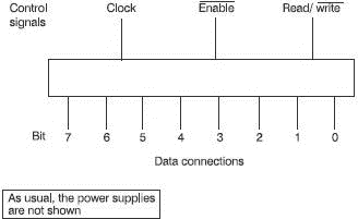
A register is just a collection of flip-flops. A flip-flop can only store one bit so to handle 32 bits at a time we would need 32 flip-flops and would refer to this as a 32-bit register. To save space, Figure 6.5 shows an 8-bit register.

Figure 6.5 An 8-bit register
The register has two distinct groups of connections: the data bits 0 to 7 and the control signals. The data connections or data lines carry the binary levels in or out of the register. The number of data lines determines the size of the register so a 64-bit register would have 64 data connections.
The three control signals include two new ones
1 Enable. This is a simple on/off switch for the register. We met this in Chapter 5 with the tri-state buffer. The line over the top of the word indicates that it is ‘on’ when this line is ‘low’ or at logic zero. We tend to say the line is ‘active low’ in this situation. Therefore, it follows that the register is disabled or switched ‘off’ when the enable line is at logic 1 or ‘high’. Nearly all control lines are active low. The benefit of having the enable line is that we are able to disconnect a register without doing any physical uncoupling of links etc.
2 Read/write. The terms ‘read’ and ‘write’ are used to describe the direction of data movement. We ‘write’ data into a register then ‘read’ the data to recover it.
You may remember that the flip-flop in Figure 6.1 included a separate line for reading the data and another for writing. Now, while this was OK with a single flip-flop, a 64-bit register would require 128 lines just to carry the data in and out. By using the tri-state buffer from Chapter 5, we can use each line to read and write data as required. The tri-state buffers are all controlled by the logic level applied to the read/write line. The normal convention applies – the line over the ‘write’ means that this line is taken low to write data and, of course, high to read data.
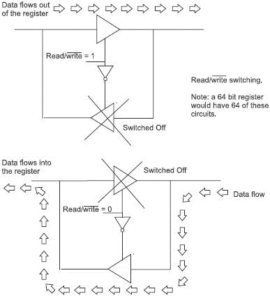
It may be interesting to look inside the register to see how the tristate buffer is used to achieve this two-way traffic on a single wire. Have a look at Figure 6.6. Two tri-state buffers are connected back-to-back. In the first example, logic 1 input will enable the top buffer. The control voltage is inverted to a logic 0, which then disables the lower buffer. Data can now flow from left to right. When the control signal changes to a logic 0, the top buffer is disabled and the lower one is enabled and the reverse direction of data flow is possible. Note how two buffers and an inverter are used for each line to be controlled. A single control line is used to switch all the data lines at the same time.

Figure 6.6 Two-way data flow
What are registers for?
Registers are storage areas inside the microprocessor. Almost the whole of the microprocessor is made of registers. They store the data that is going to be used, they store the instructions that are to be used and they store the results obtained. Nearly all registers involve tri-state buffers to control the direction of data flow.
In most cases, the data to be stored is applied to the inputs of the register and, after a short pause to let the voltages stabilize, the register is enabled by the voltage on the enable control. The information is then safely stored until it is next required.
The sequence is:
1 The read/write line is taken to logic 0 to allow the register to receive data from an external source.
2 The enable control switches ON the tri-state buffers at the input to each flip-flop.
3 The data is written to each flip-flop and then the enable control puts the register to sleep until the next time it is needed.
How long can it be stored?
It will be stored until the power supplies are removed – either by an equipment fault or, more usually, by the system being switched off. The data does not deteriorate in storage.
- A flip-flop or bistable
- A register
- Shift registers
- Rotate registers
- Memories
- RAM
- Accessing memory
- Two types of RAM
- Memory organization
- Three types of ROM
- Pin layout of an EPROM
- Pin layout of a SRAM
- Pin layout of a DRAM
- Some more memories that don’t fit into the general pattern
- Memory maps
- Quiz time 6
- Introduction to Microprocessors and Microcontrollers
- 15.6.1 Synchronous Activity Synchronization
- 12.2.1 Port-Mapped vs. Memory-Mapped I
- Assembly language, the second generation language
- Модуль RobotTaskMaker
- Your Own Domain Name and Third-Party DNS
- Providing DNS for a Real Domain
- Registering the Domain
- КЛЮЧЕВЫЕ СЛОВА: auto, extern, static, register
- 2.1.3 The Configuration Registers
- PROJECT 7.1 — Read CID Register and Display on a PC Screen
- 8.3 Event Registers


