Книга: Introduction to Microprocessors and Microcontrollers
Pin layout of an EPROM
Pin layout of an EPROM
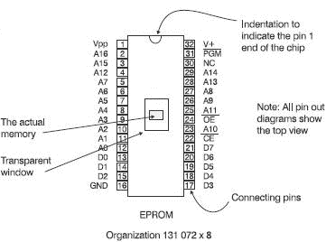
Figure 6.19 shows the pin-out diagram for a 1 Mb (1 048 576 bits) EPROM with an organization of 131 072?8 bits.

Figure 6.19 Pin out diagram of an EPROM
Power supplies
The main power supplies to operate the chip are the +5 V applied to the V+ pin and 0 V on the GND (ground) pin.
To program the memory, the programming voltage is applied to Vpp. When not being programmed, it should be held at +5 V. Be careful to read the data book – the value of Vpp differs widely.
Address pins
Address pins are always numbered starting from A0. We have seen that the number of location is given by 2nso with 17 address lines (A0 to A16) the number of locations would be 217=131 072.
Data pins
Like the addresses, these pins always start counting from zero. In the EPROM shown in Figure 6.19, they are abbreviated to D for data and go from D0 to D7 – eight in all. Some manufacturers call them output pins and number them O0, O1, O2 etc. The output from these pins is either 0 V or +5 V or near to these values.
Control pins
1 Chip enable (CE), sometimes called chip select (CS), is the main on/off switch for the chip. It is usually active low, which means that the chip needs a logic 0 voltage to be applied to switch the chip on. This is indicated by a line over the CE. When the chip is switched off, it goes to sleep and the power drops with a reduction of about 150 times.
2 Output enable (OE) leaves the chip fired up but with its output disconnected from the data pins. This is done by disabling a series of tri-state buffers immediately before the data pins. Disconnecting the output pins is very much faster than switching the chip off. Watch out for the line over the name to indicate the polarities required.
Unconnected pins
These are shown as NC and are not used. They are physically separate from the internal chip and therefore have no effect of anything. They should be left unconnected.
- A flip-flop or bistable
- A register
- Shift registers
- Rotate registers
- Memories
- RAM
- Accessing memory
- Two types of RAM
- Memory organization
- Three types of ROM
- Pin layout of an EPROM
- Pin layout of a SRAM
- Pin layout of a DRAM
- Some more memories that don’t fit into the general pattern
- Memory maps
- Quiz time 6


