Книга: Introduction to Microprocessors and Microcontrollers
A flip-flop or bistable
A flip-flop or bistable
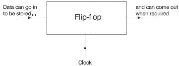
A flip-flop or bistable is a circuit that can store a single binary bit – either 0 or 1. One useful characteristic of the flip-flop is that it can only have an output of 0 or 1. It cannot hover somewhere in between. The flip-flop is shown in Figure 6.1. The purpose of the clock input is to tell the flip-flop when to accept the new input level.

Figure 6.1 A flip-flop – the basic building block of a microprocessor
The sequence of the events is:
1 Apply the binary level to be stored.
2 Wait a short time (a few nanoseconds) until the voltage is properly established.
3 Apply a signal to the clock input to tell the flip-flop to memorize the signal present at the input.
Why do we have to wait?
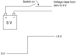
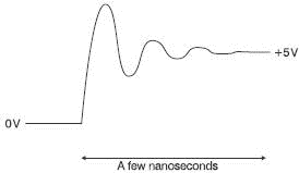
When we apply a voltage to a length of wire, we would hope that the voltage changes as in Figure 6.2. Unfortunately, it takes a few nanoseconds to settle down. The rise of voltage travels along the connecting wire and is reflected from the end causing another voltage to be reflected towards the input. This reflection is itself reflected and after repeated reflections, the voltage slowly settles down to its new level as in Figure 6.3. This occurs if we suddenly tip a bucket of water into a half-filled bath. The added water sets up a wave that is reflected backwards and forwards along the bath as the new level is established. If we didn’t wait for the voltage to settle down, we could accidentally store an incorrect value.

Figure 6.2 A voltage is switched on – how we would like it to change

Figure 6.3 A voltage is switched on – what really happens?
And what about the clock signal?
This is just an input to tell the flip-flop that it is time to read the input level. All microprocessor operations are carefully timed by clock pulses to ensure that the system operates in the correct sequence.
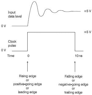
The clock signal is usually a positive-going voltage pulse. This pulse can be used to switch two circuits at different times by designing one circuit to respond to an increasing voltage and the other to use a decreasing voltage. If, for example, the pulse in Figure 6.4 were to be 10 ns wide then this could create the required delay for the voltage to settle. The circuit supplying the input voltage is kicked into action by the positive-going edge and then 10 ns later the negative-going edge instructs the flip-flop to save the data present at that time.

Figure 6.4 Using a clock pulse to control timing of a circuit
- A flip-flop or bistable
- A register
- Shift registers
- Rotate registers
- Memories
- RAM
- Accessing memory
- Two types of RAM
- Memory organization
- Three types of ROM
- Pin layout of an EPROM
- Pin layout of a SRAM
- Pin layout of a DRAM
- Some more memories that don’t fit into the general pattern
- Memory maps
- Quiz time 6


