Книга: Introduction to Microprocessors and Microcontrollers
Pin layout of a SRAM
Pin layout of a SRAM
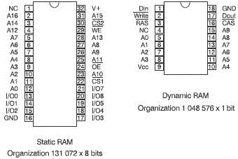
Have a look at the SRAM in Figure 6.20. Many of these pins will be recognized as being the same as we saw with the EPROM.

Figure 6.20 Pin out diagrams of RAM chips
Data pins
Since the SRAM is a read/write memory, the data pins are used to read data into the chip and to write data out to the microprocessor system. With this in mind, they have been called input/output pins (I/O) and, as usual, are numbered from zero.
Control pins
1 Write enable (WE#) controls internal tri-state buffers to control the flow of data to write or read on the data pins. The line over the WE indicates that, to write data, the pin must be held low. 2 There are two chip selects, one shown as active low and one as active high. To enable the chip, both must have the correct voltage present. This provides a degree of flexibility to the system designer. If either is not required, it can simply be held down permanently to its appropriate voltage and then the other can then be used to control the operation of the chip.
- A flip-flop or bistable
- A register
- Shift registers
- Rotate registers
- Memories
- RAM
- Accessing memory
- Two types of RAM
- Memory organization
- Three types of ROM
- Pin layout of an EPROM
- Pin layout of a SRAM
- Pin layout of a DRAM
- Some more memories that don’t fit into the general pattern
- Memory maps
- Quiz time 6


