Книга: Advanced PIC Microcontroller Projects in C
2.1.10 Capture/Compare/PWM Modules (CCP)
Разделы на этой странице:
2.1.10 Capture/Compare/PWM Modules (CCP)
The PIC18F452 microcontroller has two capture/compare/PWM (CCP) modules, and they work with Timers 1, 2, and 3 to provide capture, compare, and pulse width modulation (PWM) operations. Each module has two 8-bit registers. Module 1 registers are CCPR1L and CCPR1H, and module 2 registers are CCPR2L and CCPR2H. Together, each register pair forms a 16-bit register and can be used to capture, compare, or generate waveforms with a specified duty cycle. Module 1 is controlled by register CCP1CON, and module 2 is controlled by CCP2CON. Figure 2.34 shows the bit allocations of the CCP control registers.
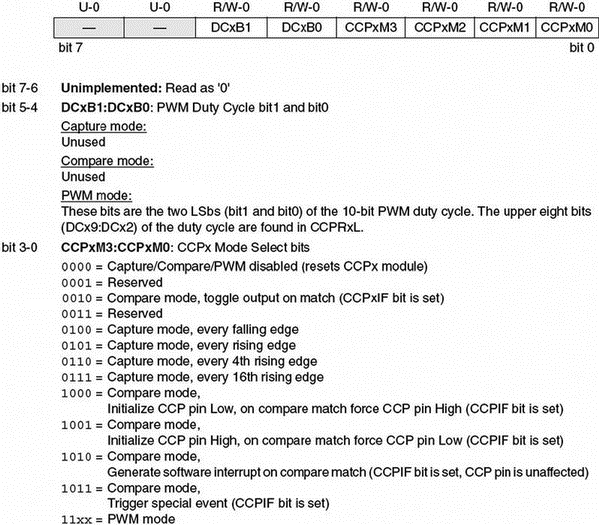
Figure 2.34: CCPxCON register bit allocations
Capture Mode
In capture mode, the registers operate like a stopwatch. When an event occurs, the time of the event is recorded, although the clock continues running (a stopwatch, on the other hand, stops when the event time is recorded).
Figure 2.35 shows the capture mode of operation. Here, CCP1 will be considered, but the operation of CCP2 is identical with the register and port names changed accordingly. In this mode CCPR1H:CCPR1L captures the 16-bit value of the TMR1 or TMR3 registers when an event occurs on pin RC2/CCP1 (pin RC2/CCP1 must be configured as an input pin using TRISC). An external signal can be prescaled by 4 or 16. The event is selected by control bits CCP1M3:CCP1M0, and any of the following events can be selected:
• Every falling edge
• Every rising edge
• Every fourth rising edge
• Every sixteenth rising edge
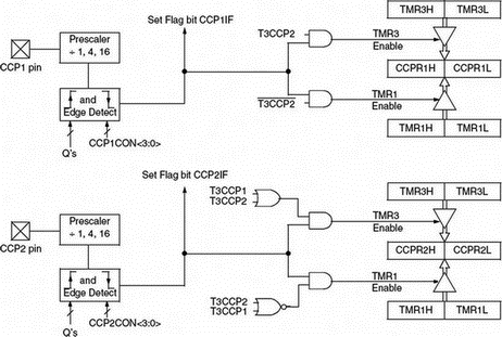
Figure 2.35: Capture mode of operation
If the capture interrupt is enabled, the occurrence of an event causes an interrupt to be generated in software. If another capture occurs before the value in register CCPR1 is read, the old captured value is overwritten by the new captured value.
Either Timer 1 or Timer 3 can be used in capture mode. They must be running in timer mode, or in synchronized counter mode, selected by register T3CON.
Compare Mode
In compare mode, a digital comparator is used to compare the value of Timer 1 or Timer 3 to the value in a 16-bit register pair. When a match occurs, the output state of a pin is changed. Figure 2.36 shows the block diagram of compare mode in operation.
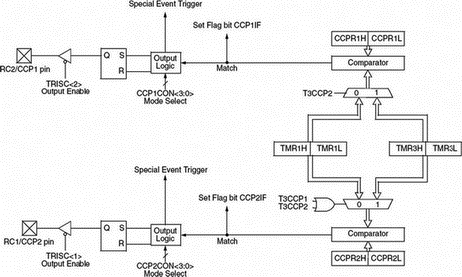
Figure 2.36: Compare mode of operation
Here only module CCP1 is considered, but the operation of module CCP2 is identical.
The value of the 16-bit register pair CCPR1H:CCPR1L is continuously compared against the Timer 1 or Timer 3 value. When a match occurs, the state of the RC2/CCP1 pin is changed depending on the programming of bits CCP1M2:CCP1M0 of register CCP1CON. The following changes can be programmed:
• Force RC2/CCP1 high
• Force RC2/CCP1 low
• Toggle RC2/CCP1 pin (low to high or high to low)
• Generate interrupt when a match occurs
• No change
Timer 1 or Timer 3 must be running in timer mode or in synchronized counter mode, selected by register T3CON.
PWM Module
The pulse width modulation (PWM) mode produces a PWM output at 10-bit resolution. A PWM output is basically a square waveform with a specified period and duty cycle. Figure 2.37 shows a typical PWM waveform.
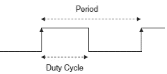
Figure 2.37: Typical PWM waveform
Figure 2.38 shows the PWM module block diagram. The module is controlled by Timer 2. The PWM period is given by:
PWM period = (PR2 + 1) * TMR2PS * 4 * TOSC (2.3)
or

where
PR2 is the value loaded into Timer 2 register
TMR2PS is the Timer 2 prescaler value
TOSC is the clock oscillator period (seconds)
The PWM frequency is defined as 1/(PWM period).
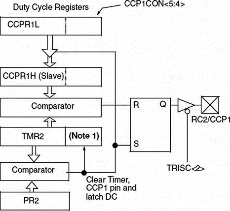
Figure 2.38: PWM module block diagram
The resolution of the PWM duty cycle is 10 bits. The PWM duty cycle is selected by writing the eight most significant bits into the CCPR1L register and the two least significant bits into bits 4 and 5 of CCP1CON register. The duty cycle (in seconds) is given by:
PWM duty cycle = (CCPR1L:CCP1CON<5:4>) * TMR2PS * TOSC (2.5)
or

The steps to configure the PWM are as follows:
• Specify the required period and duty cycle.
• Choose a value for the Timer 2 prescaler (TMR2PS).
• Calculate the value to be written into the PR2 register using Equation (2.2).
• Calculate the value to be loaded into the CCPR1L and CCP1CON registers using Equation (2.6).
• Clear bit 2 of TRISC to make CCP1 pin an output pin.
• Configure the CCP1 module for PWM operation using register CCP1CON.
The following example shows how the PWM can be set up.
Example 2.1
PWM pulses must be generated from pin CCP1 of a PIC18F452 microcontroller. The required pulse period is 44ms and the required duty cycle is 50%. Assuming that the microcontroller operates with a 4MHz crystal, calculate the values to be loaded into the various registers.
Solution 2.1
Using a 4MHz crystal; TOSC = 1/4 = 0.25 ? 10–6
The required PWM duty cycle is 44/2 = 22?s.
From Equation (2.4), assuming a timer prescaler factor of 4, we have:

or

and from Equation (2.6)

or

But the equivalent of number 22 in 10-bit binary is:
“00 00010110”
Therefore, the value to be loaded into bits 4 and 5 of CCP1CON is “00.” Bits 2 and 3 of CCP1CON must be set to high for PWM operation. Therefore, CCP1CON must be set to bit pattern (“X” is “don’t care”):
XX001100
Taking the don’t-care entries as 0, we can set CCP1CON to hexadecimal 0CH.
The value to be loaded into CCPR1L is “00010110” (i.e., hexadecimal number 16H). The required steps are summarized as follows:
• Load Timer 2 with prescaler of 4 (i.e., load T2CON) with 00000101 (i.e., 05H).
• Load 0AH into PR2.
• Load 16H into CCPR1L.
• Load 0 into TRISC (make CCP1 pin output).
• Load 0CH into CCP1CON.
One period of the generated PWM waveform is shown in Figure 2.39.
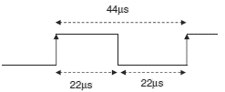
Figure 2.39: Generated PWM waveform
- 2.1.1 Program Memory Organization
- 2.1.2 Data Memory Organization
- 2.1.3 The Configuration Registers
- 2.1.4 The Power Supply
- 2.1.5 The Reset
- 2.1.6 The Clock Sources
- 2.1.7 Watchdog Timer
- 2.1.8 Parallel I/O Ports
- 2.1.9 Timers
- 2.1.10 Capture/Compare/PWM Modules (CCP)
- 2.1.11 Analog-to-Digital Converter (A/D) Module
- 2.1.12 Interrupts


