Книга: Advanced PIC Microcontroller Projects in C
2.1.6 The Clock Sources
Разделы на этой странице:
2.1.6 The Clock Sources
The PIC18F452 microcontroller can be operated from an external crystal or ceramic resonator connected to the microcontroller’s OSC1 and OSC2 pins. In addition, an external resistor and capacitor, an external clock source, and in some models internal oscillators can be used to provide clock pulses to the microcontroller. There are eight clock sources on the PIC18F452 microcontroller, selected by the configuration register CONFIG1H. These are:
• Low-power crystal (LP)
• Crystal or ceramic resonator (XT)
• High-speed crystal or ceramic resonator (HS)
• High-speed crystal or ceramic resonator with PLL (HSPLL)
• External clock with FOSC/4 on OSC2 (EC)
• External clock with I/O on OSC2 (port RA6) (ECIO)
• External resistor/capacitor with FOSC/4 output on OSC2 (RC)
• External resistor/capacitor with I/O on OSC2 (port RA6) (RCIO)
Crystal or Ceramic Resonator Operation
The first several clock sources listed use an external crystal or ceramic resonator that is connected to the OSC1 and OSC2 pins. For applications where accuracy of timing is important, a crystal should be used. And if a crystal is used, a parallel resonant crystal must be chosen, since series resonant crystals do not oscillate when the system is first powered.
Figure 2.14 shows how a crystal is connected to the microcontroller. The capacitor values depend on the mode of the crystal and the selected frequency. Table 2.4 gives the recommended values. For example, for a 4MHz crystal frequency, use 15pF capacitors. Higher capacitance increases the oscillator stability but also increases the start-up time.
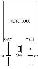
Figure 2.14: Using a crystal as the clock input
Table 2.4: Capacitor values
| Mode | Frequency | C1,C2 (pF) |
|---|---|---|
| LP | 32 KHz | 33 |
| 200 KHz | 15 | |
| XT | 200 KHz | 22–68 |
| 1.0 MHz | 15 | |
| 4.0 MHz | 15 | |
| HS | 4.0 MHz | 15 |
| 8.0 MHz | 15–33 | |
| 20.0 MHz | 15–33 | |
| 25.0 MHz | 15–33 |
Resonators should be used in low-cost applications where high accuracy in timing is not required. Figure 2.15 shows how a resonator is connected to the microcontroller.
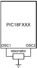
Figure 2.15: Using a resonator as the clock input
The LP (low-power) oscillator mode is advised in applications to up to 200KHz clock. The XT mode is advised to up to 4MHz, and the HS (high-speed) mode is advised in applications where the clock frequency is between 4MHz to 25MHz.
An external clock source may also be connected to the OSC1 pin in the LP, XT, or HS modes as shown in Figure 2.16.
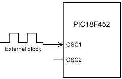
Figure 2.16: Connecting an external clock in LP, XT, or HS modes
External Clock Operation
An external clock source can be connected to the OSC1 input of the microcontroller in EC and ECIO modes. No oscillator start-up time is required after a power-on reset. Figure 2.17 shows the operation with the external clock in EC mode. Timing pulses at the frequency FOSC/4 are available on the OSC2 pin. These pulses can be used for test purposes or to provide pulses to external devices.
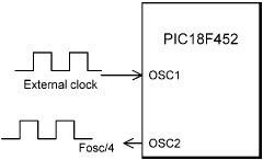
Figure 2.17: External clock in EC mode
The ECIO mode is similar to the EC mode, except that the OSC2 pin can be used as a general purpose digital I/O pin. As shown in Figure 2.18, this pin becomes bit 6 of PORTA (i.e., pin RA6).
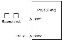
Figure 2.18: External clock in ECIO mode
Resistor/Capacitor Operation
In the many applications where accurate timing is not required we can use an external resistor and a capacitor to provide clock pulses. The clock frequency is a function of the resistor, the capacitor, the power supply voltage, and the temperature. The clock frequency is not accurate and can vary from unit to unit due to manufacturing and component tolerances. Table 2.5 gives the approximate clock frequency with various resistor and capacitor combinations. A close approximation of the clock frequency is 1/(4.2RC), where R should be between 3K and 100K and C should be greater than 20pF.
Table 2.5: Clock frequency with RC
| C (pF) | R (K) | Frequency (MHz) |
|---|---|---|
| 22 | 3.3 | 3.3 |
| 4.7 | 2.3 | |
| 10 | 1.08 | |
| 30 | 3.3 | 2.4 |
| 4.7 | 1.7 | |
| 10 | 0.793 |
In RC mode, the oscillator frequency divided by 4 (FOSC/4) is available on pin OSC2 of the microcontroller. Figure 2.19 shows the operation at a clock frequency of approximately 2MHz, where R=3.9K and C=30pF. In this application the clock frequency at the output of OSC2 is 2MHz/4=500KHz.
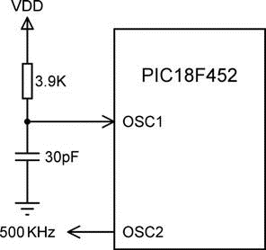
Figure 2.19: 2MHz clock in RC mode
RCIO mode is similar to RC mode, except that the OSC2 pin can be used as a general purpose digital I/O pin. As shown in Figure 2.20, this pin becomes bit 6 of PORTA (i.e., pin RA6).
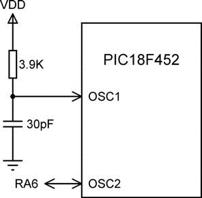
Figure 2.20: 2MHz clock in RCIO mode
Crystal or Resonator with PLL
One of the problems with using high-frequency crystals or resonators is electromagnetic interference. A Phase Locked Loop (PLL) circuit is provided that can be enabled to multiply the clock frequency by 4. Thus, for a crystal clock frequency of 10MHz, the internal operation frequency will be multiplied to 40MHz. The PLL mode is enabled when the oscillator configuration bits are programmed for HS mode.
Internal Clock
Some devices in the PIC18F family have internal clock modes (although the PIC18F452 does not). In this mode, OSC1 and OSC2 pins are available for general purpose I/O (RA6 and RA7) or as FOSC/4 and RA7. An internal clock can be from 31KHz to 8MHz and is selected by registers OSCCON and OSCTUNE. Figure 2.21 shows the bits of internal clock control registers.
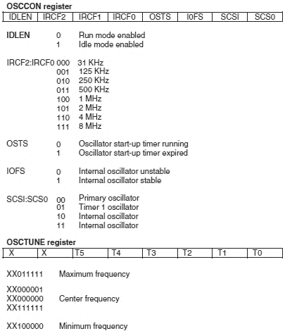
Figure 2.21: Internal clock control registers
Clock Switching
It is possible to switch the clock from the main oscillator to a low-frequency clock source. For example, the clock can be allowed to run fast in periods of intense activity and slower when there is less activity. In the PIC18F452 microcontroller this is controlled by bit SCS of the OSCCON register. In microcontrollers of the PIC18F family that do support an internal clock, clock switching is controlled by bits SCS0 and SCS1 of OSCCON. It is important to ensure that during clock switching unwanted glitches do not occur in the clock signal. PIC18F microcontrollers contain circuitry to ensure error-free switching from one frequency to another.
- 2.1.1 Program Memory Organization
- 2.1.2 Data Memory Organization
- 2.1.3 The Configuration Registers
- 2.1.4 The Power Supply
- 2.1.5 The Reset
- 2.1.6 The Clock Sources
- 2.1.7 Watchdog Timer
- 2.1.8 Parallel I/O Ports
- 2.1.9 Timers
- 2.1.10 Capture/Compare/PWM Modules (CCP)
- 2.1.11 Analog-to-Digital Converter (A/D) Module
- 2.1.12 Interrupts
- Using the date Command
- 2.1.4 The Power Supply
- 3.1.3. Clock Synchronization Algorithms
- 4.4.4 The Dispatcher
- About the author
- Chapter 7. The state machine
- Appendix E. Other resources and links
- Example NAT machine in theory
- The final stage of our NAT machine
- Compiling the user-land applications
- The conntrack entries
- Untracked connections and the raw table


