Книга: Advanced PIC Microcontroller Projects in C
2.1.8 Parallel I/O Ports
Разделы на этой странице:
2.1.8 Parallel I/O Ports
The parallel ports in PIC18F microcontrollers are very similar to those of the PIC16 series. The number of I/O ports and port pins varies depending on which PIC18F microcontroller is used, but all of them have at least PORTA and PORTB. The pins of a port are labeled as RPn, where P is the port letter and n is the port bit number. For example, PORTA pins are labeled RA0 to RA7, PORTB pins are labeled RB0 to RB7, and so on.
When working with a port we may want to:
• Set port direction
• Set an output value
• Read an input value
• Set an output value and then read back the output value
The first three operations are the same in the PIC16 and the PIC18F series. In some applications we may want to send a value to the port and then read back the value just sent. The PIC16 series has a weakness in the port design such that the value read from a port may be different from the value just written to it. This is because the reading is the actual port bit pin value, and this value can be changed by external devices connected to the port pin. In the PIC18F series, a latch register (e.g., LATA for PORTA) is introduced to the I/O ports to hold the actual value sent to a port pin. Reading from the port reads the latched value, which is not affected by any external device.
In this section we shall be looking at the general structure of I/O ports.
PORTA
In the PIC18F452 microcontroller PORTA is 7 bits wide and port pins are shared with other functions. Table 2.6 shows the PORTA pin functions.
Table 2.6: PIC18F452 PORTA pin functions
| Pin | Description |
|---|---|
| RA0/AN0 | |
| RA0 | Digital I/O |
| AN0 | Analog input 0 |
| RA1/AN1 | |
| RA1 | Digital I/O |
| AN1 | Analog input 1 |
| RA2/AN2/VREF– | |
| RA2 | Digital I/O |
| AN2 | Analog input 2 |
| VREF– | A/D reference voltage (low) input |
| RA3/AN3/VREF+ | |
| RA3 | Digital I/O |
| AN3 | Analog input 3 |
| VREF+ | A/D reference voltage (high) input |
| RA4/T0CKI | |
| RA4 | Digital I/O |
| T0CKI | Timer 0 external clock input |
| RA5/AN4/SS/LVDIN | |
| RA5 | Digital I/O |
| AN4 | Analog input 4 |
| SS | SPI Slave Select input |
| RA6 | Digital I/O |
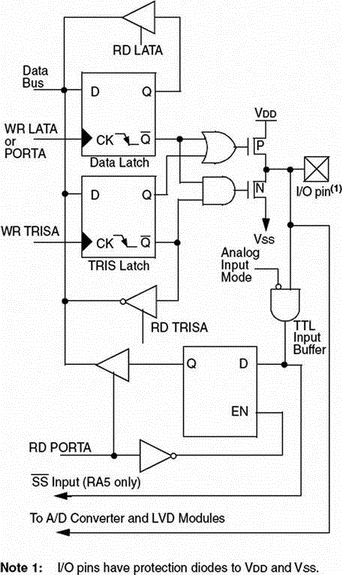
The architecture of PORTA is shown in Figure 2.22. There are three registers associated with PORTA:
• Port data register — PORTA
• Port direction register — TRISA
• Port latch register — LATA

Figure 2.22: PIC18F452 PORTA RA0–RA3 and RA5 pins
PORTA is the name of the port data register. The TRISA register defines the direction of PORTA pins, where a logic 1 in a bit position defines the pin as an input pin, and a 0 in a bit position defines it as an output pin. LATA is the output latch register which shares the same data latch as PORTA. Writing to one is equivalent to writing to the other. But reading from LATA activates the buffer at the top of the diagram, and the value held in the PORTA/LATA data latch is transferred to the data bus independent of the state of the actual output pin of the microcontroller.
Bits 0 through 3 and 5 of PORTA are also used as analog inputs. After a device reset, these pins are programmed as analog inputs and RA4 and RA6 are configured as digital inputs. To program the analog inputs as digital I/O, the ADCON1 register (A/D register) must be programmed accordingly. Writing 7 to ADCON1 configures all PORTA pins as digital I/O.
The RA4 pin is multiplexed with the Timer 0 clock input (T0CKI). This is a Schmitt trigger input and an open drain output.
RA6 can be used as a general purpose I/O pin, as the OSC2 clock input, or as a clock output providing FOSC/4 clock pulses.
PORTB
In PIC18F452 microcontroller PORTB is an 8-bit bidirectional port shared with interrupt pins and serial device programming pins. Table 2.7 gives the PORTB bit functions.
Table 2.7: PIC18F452 PORTB pin functions
| Pin | Description |
|---|---|
| RB0/INT0 | |
| RB0 | Digital I/O |
| INT0 | External interrupt 0 |
| RB1/INT1 | |
| RB1 | Digital I/O |
| INT1 | External interrupt 1 |
| RB2/INT2 | |
| RB2 | Digital I/O |
| INT2 | External interrupt 2 |
| RB3/CCP2 | |
| RB3 | Digital I/O |
| CCP2 | Capture 2 input, compare 2, and PWM2 output |
| RB4 | Digital I/O, interrupt on change pin |
| RB5/PGM | |
| RB5 | Digital I/O, interrupt on change pin |
| PGM | Low-voltage ICSP programming pin |
| RB6/PGC | |
| RB6 | Digital I/O, interrupt on change pin |
| PGC | In-circuit debugger and ICSP programming pin |
| RB7/PGD | |
| RB7 | Digital I/O, interrupt on change pin |
| PGD | In-circuit debugger and ICSP programming pin |
PORTB is controlled by three registers:
• Port data register — PORTB
• Port direction register — TRISB
• Port latch register — LATB
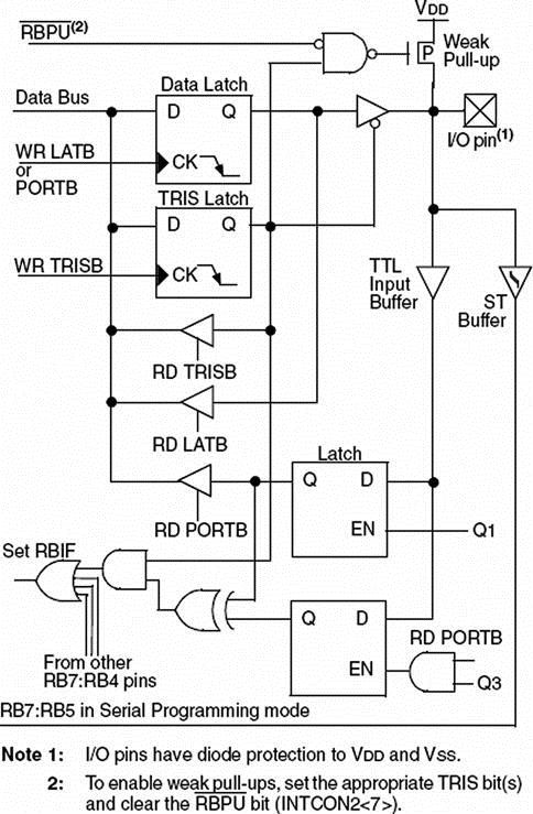
The general operation of PORTB is similar to that of PORTA. Figure 2.23 shows the architecture of PORTB. Each port pin has a weak internal pull-up which can be enabled by clearing bit RBPU of register INTCON2. These pull-ups are disabled on a power-on reset and when the port pin is configured as an output. On a power-on reset, PORTB pins are configured as digital inputs. Internal pull-ups allow input devices such as switches to be connected to PORTB pins without the use of external pull-up resistors. This saves costs because the component count and wiring requirements are reduced.

Figure 2.23: PIC18F452 PORTB RB4–RB7 pins
Port pins RB4–RB7 can be used as interrupt-on-change inputs, whereby a change on any of pins 4 through 7 causes an interrupt flag to be set. The interrupt enable and flag bits RBIE and RBIF are in register INTCON.
PORTC, PORTD, PORTE, and Beyond
In addition to PORTA and PORTB, the PIC18F452 has 8-bit bidirectional ports PORTC and PORTD, and 3-bit PORTE. Each port has its own data register (e.g., PORTC), data direction register (e.g., TRISC), and data latch register (e.g., LATC). The general operation of these ports is similar to that of PORTA.2.1.
In the PIC18F452 microcontroller PORTC is multiplexed with several peripheral functions as shown in Table 2.8. On a power-on reset, PORTC pins are configured as digital inputs.
Table 2.8: PIC18F452 PORTC pin functions
| Pin | Description |
|---|---|
| RC0/T1OSO/T1CKI | |
| RC0 | Digital I/O |
| T1OSO | Timer 1 oscillator output |
| T1CKI | Timer 1/Timer 3 external clock input |
| RC1/T1OSI/CCP2 | |
| RC1 | Digital I/O |
| T1OSI | Timer 1 oscillator input |
| CCP2 | Capture 2 input, Compare 2 and PWM2 output |
| RC2/CCP1 | |
| RC2 | Digital I/O |
| CCP1 | Capture 1 input, Compare 1 and PWM1 output |
| RC3/SCK/SCL | |
| RC3 | Digital I/O |
| SCK | Synchronous serial clock input/output for SPI |
| SCL | Synchronous serial clock input/output for I?C |
| RC4/SDI/SDA | |
| RC4 | Digital I/O |
| SDI | SPI data in |
| SDA | I?C data I/O |
| RC5/SDO | |
| RC5 | Digital I/O |
| SDO | SPI data output |
| RC6/TX/CK | |
| RC6 | Digital I/O |
| TX | USART transmit pin |
| CK | USART synchronous clock pin |
| RC7/RX/DT | |
| RC7 | Digital I/O |
| RX | USART receive pin |
| DT | USART synchronous data pin |
In the PIC18F452 microcontroller, PORTD has Schmitt trigger input buffers. On a power-on reset, PORTD is configured as digital input. PORTD can be configured as an 8-bit parallel slave port (i.e., a microprocessor port) by setting bit 4 of the TRISE register. Table 2.9 shows functions of PORTD pins.
Table 2.9: PIC18F452 PORTD pin functions
| Pin | Description |
|---|---|
| RD0/PSP0 | |
| RD0 | Digital I/O |
| PSP0 | Parallel slave port bit 0 |
| RD1/PSP1 | |
| RD1 | Digital I/O |
| PSP1 | Parallel slave port bit 1 |
| RD2/PSP2 | |
| RD2 | Digital I/O |
| PSP2 | Parallel slave port bit 2 |
| RD3/PSP3 | |
| RD3 | Digital I/O |
| PSP3 | Parallel slave port bit 3 |
| RD4/PSP4 | |
| RD4 | Digital I/O |
| PSP4 | Parallel slave port bit 4 |
| RD5/PSP5 | |
| RD5 | Digital I/O |
| PSP5 | Parallel slave port bit 5 |
| RD6/PSP6 | |
| RD6 | Digital I/O |
| PSP6 | Parallel slave port bit 6 |
| RD7/PSP7 | |
| RD7 | Digital I/O |
| PSP7 | Parallel slave port bit 7 |
In the PIC18F452 microcontroller, PORTE is only 3 bits wide. As shown in Table 2.10, port pins are shared with analog inputs and with parallel slave port read/write control bits. On a power-on reset, PORTE pins are configured as analog inputs and register ADCON1 must be programmed to change these pins to digital I/O.
Table 2.10: PIC18F452 PORTE pin functions
| Pin | Description |
|---|---|
| RE0/RD/AN5 | |
| RE0 | Digital I/O |
| RD | Parallel slave port read control pin |
| AN5 | Analog input 5 |
| RE1/WR/AN6 | |
| RE1 | Digital I/O |
| WR | Parallel slave port write control pin |
| AN6 | Analog input 6 |
| RE2/CS/AN7 | |
| RE2 | Digital I/O |
| CS | Parallel slave port CS |
| AN7 | Analog input 7 |
- 2.1.1 Program Memory Organization
- 2.1.2 Data Memory Organization
- 2.1.3 The Configuration Registers
- 2.1.4 The Power Supply
- 2.1.5 The Reset
- 2.1.6 The Clock Sources
- 2.1.7 Watchdog Timer
- 2.1.8 Parallel I/O Ports
- 2.1.9 Timers
- 2.1.10 Capture/Compare/PWM Modules (CCP)
- 2.1.11 Analog-to-Digital Converter (A/D) Module
- 2.1.12 Interrupts
- 2.2.5. ATM Switching
- Глава 2 Виртуальные машины Virtual PC 2004
- Глава 3 Виртуальные машины VMware Workstation
- Глава 4 Виртуальные машины Parallels Workstation
- Internet Workstation
- Директива parallel for
- Putting Samba to Work
- Managing Print Jobs
- Using USB and Legacy Printers
- Using xconfig to Configure the Kernel
- 2.1 PIC18FXX2 Architecture
- 2.1.8 Parallel I


