Книга: Advanced PIC Microcontroller Projects in C
2.1.2 Data Memory Organization
2.1.2 Data Memory Organization
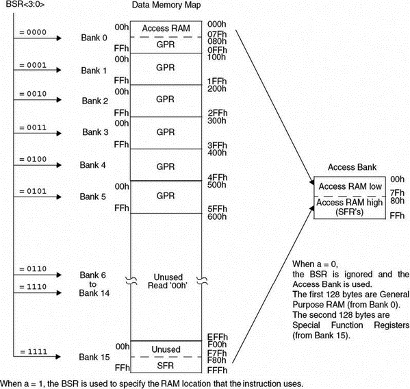
The data memory map of the PIC18F452 microcontroller is shown in Figure 2.4. The data memory address bus is 12 bits with the capability to address up to 4Mbytes. The memory in general consists of sixteen banks, each of 256 bytes, where only 6 banks are used. The PIC18F452 has 1536 bytes of data memory (6 banks ? 256 bytes each) occupying the lower end of the data memory. Bank switching happens automatically when a high-level language compiler is used, and thus the user need not worry about selecting memory banks during programming.

Figure 2.4: The PIC18F452 data memory map
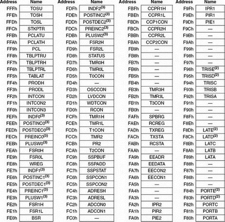
The special function register (SFR) occupies the upper half of the top memory bank. SFR contains registers which control operations such as peripheral devices, timers/counters, A/D converter, interrupts, and USART. Figure 2.5 shows the SFR registers of the PIC18F452 microcontroller.

Figure 2.5: The PIC18F452 SFR registers
- 2.1.1 Program Memory Organization
- 2.1.2 Data Memory Organization
- 2.1.3 The Configuration Registers
- 2.1.4 The Power Supply
- 2.1.5 The Reset
- 2.1.6 The Clock Sources
- 2.1.7 Watchdog Timer
- 2.1.8 Parallel I/O Ports
- 2.1.9 Timers
- 2.1.10 Capture/Compare/PWM Modules (CCP)
- 2.1.11 Analog-to-Digital Converter (A/D) Module
- 2.1.12 Interrupts
- 2.1.1 Program Memory Organization
- Memory Analyzer (Formerly MemScope)
- Класс MEMORY
- Memory Overhead
- Detect Memory Leaks
- Информация заголовочной страницы (Database header)
- Database dialect
- EVENT MEMORY SIZE
- DATABASE CACHE SIZE
- Data sending and control session
- SCTP DATA chunk
- Data Binding Using the GridView Control


