Книга: Advanced PIC Microcontroller Projects in C
2.1.9 Timers
2.1.9 Timers
The PIC18F452 microcontroller has four programmable timers which can be used in many tasks, such as generating timing signals, causing interrupts to be generated at specific time intervals, measuring frequency and time intervals, and so on.
This section introduces the timers available in the PIC18F452 microcontroller.
Timer 0
Timer 0 is similar to the PIC16 series Timer 0, except that it can operate either in 8-bit or in 16-bit mode. Timer 0 has the following basic features:
• 8-bit or 16-bit operation
• 8-bit programmable prescaler
• External or internal clock source
• Interrupt generation on overflow
Timer 0 control register is T0CON, shown in Figure 2.24. The lower 6 bits of this register have similar functions to the PIC16-series OPTION register. The top two bits are used to select the 8-bit or 16-bit mode of operation and to enable/disable the timer.
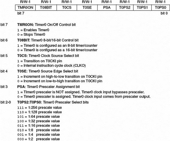
Figure 2.24: Timer 0 control register, T0CON
Timer 0 can be operated either as a timer or as a counter. Timer mode is selected by clearing the T0CS bit, and in this mode the clock to the timer is derived from FOSC/4. Counter mode is selected by setting the T0CS bit, and in this mode Timer 0 is incremented on the rising or falling edge of input RA4/T0CKI. Bit T0SE of T0CON selects the edge triggering mode.
An 8-bit prescaler can be used to change the timer clock rate by a factor of up to 256. The prescaler is selected by bits PSA and T0PS2:T0PS0 of register T0CON.
8-Bit Mode Figure 2.25 shows Timer 0 in 8-bit mode. The following operations are normally carried out in a timer application:
• Clear T0CS to select clock FOSC/4
• Use bits T0PS2:T0PS0 to select a suitable prescaler value
• Clear PSA to select the prescaler
• Load timer register TMR0L
• Optionally enable Timer 0 interrupts
• The timer counts up and an interrupt is generated when the timer value overflows from FFH to 00H in 8-bit mode (or from FFFFH to 0000H in 16-bit mode)

Figure 2.25: Timer 0 in 8-bit mode
By loading a value into the TMR0 register we can control the count until an overflow occurs. The formula that follows can be used to calculate the time it will take for the timer to overflow (or to generate an interrupt) given the oscillator period, the value loaded into the timer, and the prescaler value:
Overflow time = 4 ? TOSC ? Prescaler ? (256–TMR0) (2.1)
where
Overflow time is in ms
TOSC is the oscillator period in ?s
Prescaler is the prescaler value
TMR0 is the value loaded into TMR0 register
For example, assume that we are using a 4MHz crystal, and the prescaler is chosen as 1:8 by setting bits PS2:PS0 to 010. Also assume that the value loaded into the timer register TMR0 is decimal 100. The overflow time is then given by:
4MHZ clock has a period; T = 1/f = 0.25 ?s
using the above formula
Overflow time = 4 ? 0.25 ? 8 ? (256 – 100) = 1248 ?s
Thus, the timer will overflow after 1.248 msec, and a timer interrupt will be generated if the timer interrupt and global interrupts are enabled.
What we normally want is to know what value to load into the TMR0 register for a required overflow time. This can be calculated by modifying Equation (2.1) as follows:
TMR0 = 256 – (Overflow time)/(4 ? TOSC ? Prescaler) (2.2)
For example, suppose we want an interrupt to be generated after 500ms and the clock and the prescaler values are as before. The value to be loaded into the TMR0 register can be calculated using Equation (2.2) as follows:
TMR0 = 256 – 500/(4 ? 0.25 ? 8) = 193.5
The closest number we can load into TMR0 register is 193.
16-Bit Mode The Timer 0 in 16-bit mode is shown in Figure 2.26. Here, two timer registers named TMR0L and TMR0 are used to store the 16-bit timer value. The low byte TMR0L is directly loadable from the data bus. The high byte TMR0 can be loaded through a buffer called TMR0H. During a read of TMR0L, the high byte of the timer (TMR0) is also loaded into TMR0H, and thus all 16 bits of the timer value can be read. To read the 16-bit timer value, first we have to read TMR0L, and then read TMR0H in a later instruction. Similarly, during a write to TMR0L, the high byte of the timer is also updated with the contents of TMR0H, allowing all 16 bits to be written to the timer. Thus, to write to the timer the program should first write the required high byte to TMR0H. When the low byte is written to TMR0L, then the value stored in TMR0H is automatically transferred to TMR0, thus causing all 16 bits to be written to the timer.
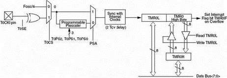
Figure 2.26: Timer 0 in 16-bit mode
Timer 1
PIC18F452 Timer 1 is a 16-bit timer controlled by register T1CON, as shown in Figure 2.27. Figure 2.28 shows the internal structure of Timer 1.
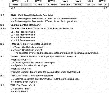
Figure 2.27: Timer 1 control register, T1CON
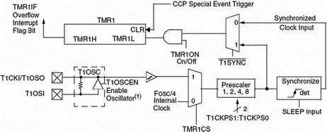
Figure 2.28: Internal structure of Timer 1
Timer 1 can be operated as either a timer or a counter. When bit TMR1CS of register T1CON is low, clock FOSC/4 is selected for the timer. When TMR1CS is high, the module operates as a counter clocked from input T1OSI. A crystal oscillator circuit, enabled from bit T1OSCEN of T1CON, is built between pins T1OSI and T1OSO where a crystal up to 200KHz can be connected between these pins. This oscillator is primarily intended for a 32KHz crystal operation in real-time clock applications. A prescaler is used in Timer 1 that can change the timing rate as a factor of 1, 2, 4, or 8.
Timer 1 can be configured so that read/write can be performed either in 16-bit mode or in two 8-bit modes. Bit RD16 of register T1CON controls the mode. When RD16 is low, timer read and write operations are performed as two 8-bit operations. When RD16 is high, the timer read and write operations are as in Timer 0 16-bit mode (i.e., a buffer is used between the timer register and the data bus) (see Figure 2.29).
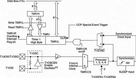
Figure 2.29: Timer 1 in 16-bit mode
If the Timer 1 interrupts are enabled, an interrupt will be generated when the timer value rolls over from FFFFH to 0000H.
Timer 2
Timer 2 is an 8-bit timer with the following features:
• 8-bit timer (TMR2)
• 8-bit period register (PR2)
• Programmable prescaler
• Programmable postscaler
• Interrupt when TM2 matches PR2
Timer 2 is controlled from register T2CON, as shown in Figure 2.30. Bits T2CKPS1:T2CKPS0 set the prescaler for a scaling of 1, 4, and 16. Bits TOUTPS3:TOUTPS0 set the postscaler for a scaling of 1:1 to 1:16. The timer can be turned on or off by setting or clearing bit TMR2ON.
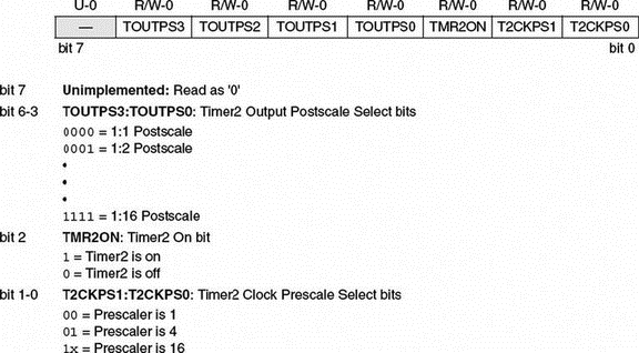
Figure 2.30: Timer 2 control register, T2CON
The block diagram of Timer 2 is shown in Figure 2.31. Timer 2 can be used for the PWM mode of the CCP module. The output of Timer 2 can be software selected by the SSP module as a baud clock. Timer 2 increments from 00H until it matches PR2 and sets the interrupt flag. It then resets to 00H on the next cycle.
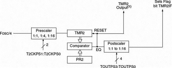
Figure 2.31: Timer 2 block diagram
Timer 3
The structure and operation of Timer 3 is the same as for Timer 1, having registers TMR3H and TMR3L. This timer is controlled from register T3CON as shown in Figure 2.32.
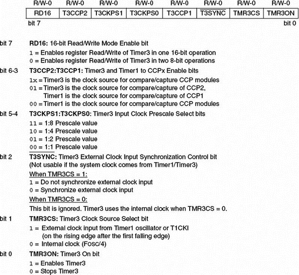
Figure 2.32: Timer 3 control register, T3CON
The block diagram of Timer 3 is shown in Figure 2.33.
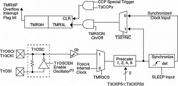
Figure 2.33: Block diagram of Timer 3
- 2.1.1 Program Memory Organization
- 2.1.2 Data Memory Organization
- 2.1.3 The Configuration Registers
- 2.1.4 The Power Supply
- 2.1.5 The Reset
- 2.1.6 The Clock Sources
- 2.1.7 Watchdog Timer
- 2.1.8 Parallel I/O Ports
- 2.1.9 Timers
- 2.1.10 Capture/Compare/PWM Modules (CCP)
- 2.1.11 Analog-to-Digital Converter (A/D) Module
- 2.1.12 Interrupts


