Книга: Introduction to Microprocessors and Microcontrollers
The PIC16F84A
The PIC16F84A
This is another modern RISC development and has many features that are similar to the AVR that we have just looked at. The AT90S/LS2343 was chosen as representative of the very small and basic microcontrollers found embedded in many products. This PIC16F84A example from Microchip Technology is a mid-range device which is larger and more capable than the AVR.
The PIC series ranges from a really simple 8-pin, 4 MHz microcontroller on a level with the AT90S/LS2343 that we have just considered up to a 40-pin 25 MHz device. As mentioned the PIC16F84A is a mid-size version that has 18 pins and runs up to 20 MHz.
The PICs are designed for easy use and are becoming increasingly popular as the first step into the world of microcontrollers. Microchip Technology provides a PICSTART™ PIC development system that provides, at a very reasonable price, an assembler, compiler, EPROM and EEPROM programmer, all the hardware manuals and even a sample PIC to play with. It should be mentioned that other companies have similar systems compatible with the PIC series and for other microcontrollers like the AVR and 8051 series.
It has proved to be such an easy, off the shelf, starting point that to many people ‘PIC’ is not only their first choice but is becoming used as a generic term for any microcontroller.
The general layout of the PIC16F84A is shown in Figure 15.7.
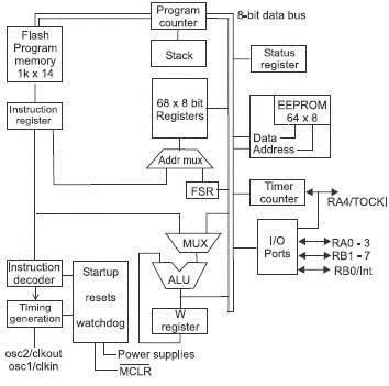
Figure 15.7 PIC16F84A
Supply voltage
The DC supply voltage must remain in the range 2.0–5.5 V for it to work happily though similar versions such as the PIC16F84 can run between 2.0 and 6.0 V.
Sleep mode
To save the current drain, a software instruction can put the PIC into a sleep mode. The supply current is very dependent on the clock frequency and is normally between 1 and 20 mA and when put to sleep the drain is reduced to approximately 1 µA. To obtain the lowest possible sleep current we should hold all I/O pins at VDD or VSS and disable any external clock and hold the master clear pin in a logic high state – not in the reset state. The purpose of all this is to prevent any voltages from floating up and down. If it did so, it would switch and the technology used results in very low currents drawn except at the moment of switching during which it causes a really high spike of current so the higher the frequency, the more often this spike occurs – hence the increased current.
The microprocessor will wake if: a reset occurs by a logic low voltage being applied to the MCLR pin, a wakeup pulse arrives from the watchdog unit (if it is enabled) or an ‘EEPROM write complete’ signal.
Memory
As usual, we have two blocks of memory. One is the program memory and the other is for data. For maximum speed, they each have a separate bus connection so that both memories can be accessed during a single clock cycle.
Program memory
The program memory is situated in the flash memory which is organized as 1028?14. All instructions in the PIC16 series use 14-bit instructions.
The reset vector points to address 0000H and the interrupt vector is 0004H so address locations 0005H to 03FFH are available for us to hold our programs.
Data memory
The data area is subdivided into two areas, the FSR (file select register) and the GP (general purpose registers) as shown in Figure 15.8.
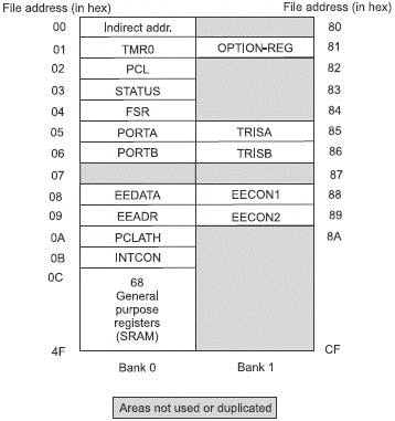
Figure 15.8 Register file map
The SFR (special function register)
This register controls the operation of the CPU and involves such things as the input and output ports, EEPROM address and data, timer, program counter and that sort of housekeeping.
All the register files are 8-bits wide and are arranged in two banks called bank 0 and bank 1. We have to instruct the microcontroller as to which bank is to be used and this is done by using special instructions to access some of the page 1 registers. Those accessible are indicated in Figure 15.8. Microchip Technology are planning to remove the choice of using the OPTION and the two TRIS registers and suggest that the STATUS register is used instead. This does not affect the use with this chip but it will ensure that upgrading in the future will not require any modifications to the software.
I/O (input/output) ports
All outputs can source or sink 25 mA and can therefore power significant external circuits without further power amplifiers being required. Sinking means that the load is connected between the positive Vcc supply and a low voltage output at the port and sourcing is connecting the load between a positive output on the pin to the ground.
PortA and TRISA registers
PortA is a 5-bit wide bi-directional port, each line being individually controlled so some of the lines can be inputs whilst the others are outputs. The choice of input or output is made by loading a 0 (output) or a 1 (input) into the appropriate bit of the data direction register TRISA.
In common with other devices, when it first starts at power-on, the port is set as an input. This provides a safer option that running the risk of random information being sent out to whatever it is connected to.
PortB and TRISB registers
PortB is a 8-bit wide bi-directional port, each line being individually controlled using TRISB in the same manner as in PortA. Each of the PortB pins have a weak internal pull-up which can be switched on or off by the RBPU of the option register. The pull-ups are disabled when the port is being used as an output and also during power switchon. Any of the Pins RB4–RB7 that just happen to be configured as an input have an interrupt-on-change feature that can be useful. If any one or more of these pins have changed logic state since they were last read, it causes an RB port change interrupt. This interrupt can be used to wake the microcontroller from its ‘sleep’ mode.
Status register
This is very similar to the one we met when looking at the Z80 in Chapter 8.
The bits are:
Bit 0 is the C(carry/borrow) bit. 1 = a carry out from the MSB (most significant bit) of the result otherwise it is cleared to zero. For ‘borrow’ the values are reversed. Subtraction is carried out using the two’s-complement method that we met in Chapter 4.
Bit 1 reflects the carry situation that last occurred from the 4th bit of the result. This is also called the half-carry bit.
Bit 2 is the zero flag. It is set to ONE when the result of the last arithmetic or logic operation is ZERO. Be careful not to misread this.
Bit 3 goes to 0 after running the SLEEP instruction.
Bit 4 goes to 0 when a watchdog time-out has occurred.
Bit 5 is used to select between the two memory banks. It is cleared to 0 to access Bank 0 and set to 1 if we need access to Bank 1.
Bit 6 and bit 7 – not used. It will be used in the future so by programming them for 0, future compatibility will be assured. This may save a lot of time if our program is used on an upgraded version.
Option register
As the name suggests, it offers a series of options. One example is the control of the prescaler.
The Prescaler
Two functions are affected by the prescaler, they are the timer, TMR0 (timer zero) and the watchdog timer. Each of these circuits provides an output pulse after the count overflows and restarts from zero. In the case of the watchdog, the time interval is about 18 ms. If a longer time interval is needed, we have three alternatives. We can simply switch the watchdog off but, of course, we lose the benefits of the watchdog if the microcontroller gets caught in a loop. A simple way is to place the software code CLRWDT (clear watchdog timer) in the program at anytime before the end of the countdown so it is reset for another 18 ms and we can repeat this as necessary. Lastly, we can use the prescaler to reduce the frequency of the incoming pulses and hence increase the time before the output signal is generated.
Bits 0, 1 and 2 PS2:PS0 (prescaler rate select bits) provide eight alternative pulse rates for use by the watchdog or TMR0. Setting the three inputs to 000 will provide a clock signal which is equal to an external signal or chip oscillator. Changing the setting to 001 will halve the frequency (or double the time). Increasing the setting to 010 will decrease the frequency to one quarter of the original. As the count increases, the frequency will halve for each count until we reach the maximum bit value of 111 which will cause the watchdog time to increase by a factor of 128. As it happens, the TMR0 has a divide by two circuit built in all the time so a setting of 000 will halve the frequency and the maximum count will reduce the frequency by a factor of 256.
Bit 3 PSA – (prescaler assignment bit) – Unlike most other PICs, the prescaler can be applied to the TMR0 or the watchdog, but NOT both, so the option register controls the choice. Bit 3 of the option register is set to 0 to prescale the TMR0 and a 1 selects the watchdog.
The other bits
Bit 4 T0SE (TMR0 source edge select). This controls the moment of timing the clock input. A ‘0’ increments the count on the low-to-high transition and a ‘1’ increments on the high-to-low transition.
Bit 5 T0CS (TMR0 clock source select). This decides where the clock pulses come from. The choices are a ‘0’ to an internal clock as on the CLKOUT pin and a ‘1’ counts the transitions on the RA4/T0CKI (timer zero clock input). This option allows pulses to be generated by any external source like cans of beans moving along the conveyor belt or the revolutions of an engine.
Bit 6 INTEDG (interrupt edge select). This is similar to bit 4 except we are controlling the moment at which an interrupt signal is recognized of the RB0/INT pin. A ‘0’ uses the falling voltage edge and a ‘1’ sets the rising edge.
Bit 7 RBPU (PortB pull-up enable). This controls the ‘pull-ups’ on the PORTB output. A ‘0’ allows each line to have its own pull-up enabled or switched off as required. A ‘1’ switches them all off. A pull-up circuit is shown in Figure 15.9. When the switch is closed by applying a ‘0’ state to this pin it connects the output to the positive supply via a current limiting resistor. This ensures that in the absence of any input data the port will be pulled up to a positive state so that it doesn’t wander about applying unpredictable inputs. The higher the value of the resistance used, the easier an incoming voltage finds it to bring the voltage down and this is referred to as a ‘weak’ pull-up like this one. Likewise, a reduction in the resistance value will make the port input more determined to stay high and this is referred to as a ‘strong’ pull-up.
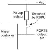
Figure 15.9 A pull-up circuit
PCL (program counter low)
PC is the program counter that keeps track of the instruction being executed at the time. It is a 13-bit register divided into PCL for low byte and PCH for high byte. Its behaviour is common with other microcontrollers and microprocessors as described in Chapter 8.
Stack
This register stores the return address when interrupts occur. It stores up to eight 13-bit addresses. Again, there are more details in Chapter 8.
Register 6–1: PIC16F84A configuration word
This is a special register which is just memory location 2007H which can only be accessed during programming. Unprogrammed pins are read as ‘1’.
It is a 13-bit word with the following options:
Bit 13–4. This protects the program code from being read after the programming is complete. 1 = no protection 0 = all program memory is code protected.
Bit 3 Power-up timer enabling. This allows a nominal 72 ms delay when first switching the microcontroller on to allow power supplies to settle. The delay can be activated by loading bit 3 with ‘0’, no delay = ‘1’.
Bit 2 watchdog timer, disable with ‘0’, enable with ‘1’.
Bits 1–0 oscillator selection bits
00 = LP oscillator
01 = HS oscillator
10 = XT oscillator
11 = RC oscillator
Oscillators
The crystal or ceramic resonator options are shown in Figure 15.10 and the crystal oscillators are divided into the frequency ranges:
LP low power crystals 32 kHz–200 kHz.
XT crystal/ceramic resonator 100 kHz–4 MHz.
HS high speed crystal/ceramic resonator 4 MHz–20 MHz.
RC resistor/capacitor.
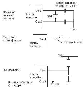
Figure 15.10 Oscillator options
A note on ceramic resonators
These offer an alternative to crystals for oscillators. They are generally lighter, more shock resistant and are usually somewhat smaller and cheaper to buy. The downside is that they do not have quite the frequency accuracy or stability and in many respects they are positioned somewhere between an RC network and the quartz crystal.
An interrupt summary
The PIC16F84A has four sources of interrupts:
(i) External interrupt on the RB0/INT pin.
(ii) TMR0 overflow.
(iii) PortB change detector pins RB7–RB4
(iv) EEPROM data write complete interrupt. This is used only when we are loading new programs into the EEPROM.
- 8.5.2 Typical Condition Variable Operations
- Introduction to Microprocessors and Microcontrollers
- Translation
- Tos match
- The echo command
- It’s All The Same, Just Different
- 11.7 Soft Timers and Timer Related Operations
- Searches
- DirectX Tutorial 2: Drawing a Polygon
- Internet Relay Chat
- Handheld Digital Cameras
- Reference
