Книга: Introduction to Microprocessors and Microcontrollers
How the system works
How the system works
In the beginning
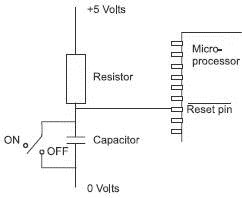
After the power supplies are first switched on, there is a short delay built in to allow the voltages to settle and for the clock to start. This delay is produced by a circuit similar to that shown in Figure 8.9.

Figure 8.9 The ON/OFF switch
The circuit uses a capacitor. A capacitor is a device designed to store electricity rather like a bucket can be filled with water.
When the micro system is switched off, the capacitor has a short circuit across it and the current that is flowing through the resistor bypasses the capacitor hence there is no electricity stored and hence there is no voltage across it. The same effect is achieved by holding the reset pin at zero volts for a time equivalent to at least six clock cycles.
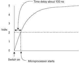
Then we switch on and the current flowing through the resistor now accumulates in the capacitor and the voltage starts to increase. The voltage grows in the way shown in Figure 8.10 and after a short period of time, less than a microsecond, the voltage reaches two volts, which is enough to switch the microprocessor on.
The clock starts ticking and the microprocessor follows a sequence of steps called a start-up microprogram that was built into the microprocessor by the manufacturer.
It performs some internal tests and similar housekeeping jobs and then puts an address on the address bus. This address is, reasonably enough, called the startup address and is again fixed by the manufacturer. In the Z80180 the startup address happens to be 0000H and so this part of the memory map must contain some ROM to hold the start-up program.

Figure 8.10 Generating a short delay when switching on
Back at Figure 6.22 we saw a typical memory map in which the startup program was held in the high end of the memory. The Z80180 would require a quite different map and this indicates yet another incompatibility between microprocessors.
The first instruction
The startup address is read by the address decoder. The decoder then applies a chip select signal on the Control bus. This signal then selects a ROM chip. All other chips ignore the signal since they have not been selected. The address enters the ROM chip and the row and address decoders access a memory cell. The contents of that cell are put on the data bus to be read by the microprocessor.
The second read
The microprocessor sends out the next address onto the address bus. The address decoder will activate the ROM chip again. The ROM chip will put some more data on the data bus, which will again be read by the microprocessor.
What does the microprocessor do with all this data?
If the first read of the ROM resulted in the data C0H and the second read produced 86H, the microprocessor combines the two to produce a 16-bit address, C086H. Remember that all this will be in binary – the use of hex is just to help us see what is happening. The microprocessor places this new address C086H on the address bus. The choice of C086H is not made by the microprocessor designer.
This number is chosen by the system designer – that is, the person that incorporates the microprocessor into a microsystem.
Then what?
The address, C086H in our example, accesses a ROM chip, which sends a binary number back to the microprocessor along the data bus. Inside the microprocessor, this number is interpreted as an instruction. Comparing the incoming number with an internal list of built-in control codes discovers exactly what the instruction is. This is all performed by the micro-program.
What happens next will depend on what the instruction was.
Why?
Why was it an instruction? Because the microprocessor said so!
Microprocessors assume that the first binary number that arrives represents an instruction so if we wanted to give it the instruction ADD 25H then the binary code meaning ADD will go in first, followed by the data to be used, in this case 25H.
What if we made a mistake and put the 25 in first, followed by the binary code for ADD in our program?
The microprocessor would interpret the 25 as an instruction – which could mean anything at all, or nothing. If this mystery instruction needed a number, it would use the binary equivalent of our ADD input – which again could be anything. If the false instruction did not need a number, then ADD instruction would be correctly read as an ADD instruction but it would then take the next available binary input as the number to be added. Our microprocessor has now carried out an incorrect instruction using incorrect data and the program could do almost anything. The whole program has got out of step and may do something quite unexpected. Not much fun in our dynamite factory.
The address being used at any time is known to the microprocessor by referring to the current value in the program counter, which is increased by one every time an instruction or some data is used.
- Configuring Wireless Networks
- 4.2.1. The Workstation Model
- 5.4.2 The Cross-Development Environment
- 4.4.4 The Dispatcher
- About the author
- How to read
- Chapter 7. The state machine
- Chapter 9. How a rule is built
- Appendix E. Other resources and links
- How it was written
- How to plan an IP filter
- Example NAT machine in theory


