Книга: Introduction to Microprocessors and Microcontrollers
Inside of the central processing unit (CPU)
Inside of the central processing unit (CPU)
Figure 8.1 shows the main parts of the Z80180 CPU. It consists of a number of different registers which store or make use of the data when carrying out the instructions in the program. In order to maintain backward compatibility, most of the registers use the same system of labelling with letters to keep it familiar to anyone who has used the Z80.
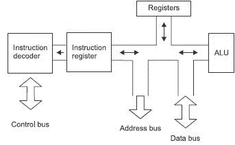
Figure 8.1 The central processing unit (CPU)
Instruction register
The instruction register is just a small memory able to store 8 bits, or 1 byte of information. This information is an instruction for the microprocessor to carry out. The information is latched into the instruction register to release the internal data bus for other purposes. It doesn’t do anything with the binary input – it just remembers what it is.
Instruction decoder
The instruction decoder is the part of the microprocessor that is able to actually carry out an instruction. Its first step is to identify which instruction that has been entered. It does this by comparing its binary code with an internally stored list. Once it has located the instruction it follows a built-in program called a microprogram. This microprogram is designed into the microprocessor by the manufacturer and details all the necessary steps to complete any instruction of which it is capable. This is the commercially sensitive and critical part of the microprocessor.
When the Z80180 is given a job to do, it must be given an instruction. An instruction is in the form of an 8-bit binary number. We will be coming back to this in a little while.
Arithmetic and logic unit (ALU)
This is a simple pocket calculator. It can add, subtract, multiply, divide, and do various tricks with logic gates AND, OR, XOR etc. Compared with the average scientific calculator, it is pretty poor.
CPU register banks
Technical information about a microprocessor will always include a diagram or listing of the internal registers. Registers are small memories, of between 8 and 128 bits each, depending on the microprocessor being considered. In the Z80180, they are all 8 or 16 bits in size.
Each microprocessor has its own collection of registers so it is essential to read the technical information carefully to see what they do.
There are ‘general purpose registers’ that are under the control of the user and can be used for a variety of temporary storage purposes.
There are also special purpose registers that are dedicated to particular functions, like the instruction register, for instance.
The Z80180 has sixteen general-purpose registers, and six for special purposes. Figure 8.2 shows the registers.
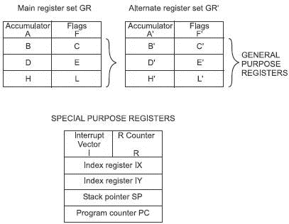
Figure 8.2 Z80X80 internal registers
We will concentrate on the upper two registers for the moment. The Main register set and the alternate register set are identical except for the small ‘ against the letters. This ‘ is called ‘prime’ so D’ would be read as ‘dee prime’. The prime is only there to distinguish between the two sets of registers.
Why have two sets? Having two sets allows the programmer to use the main set of registers while the prime registers can be loaded with other information ready for immediate use when required.
Imagine the microprocessor is busily controlling a printing machine when the fire alarm is activated. When the fire alarm signal reaches the microprocessor, it immediately abandons the printing program and starts to run the ‘Fire Alarm’ program alerting the fire fighters, evaluating the building etc. Some of the information for running this program could be stored in the spare set of registers. When the alarm program has been completed, the microprocessor calmly switches back to its main register set, and continues its printing work until it melts in the fire.
The accumulator
The programmer can use it at any time to store an 8-bit binary number. It can also store numbers to be used in arithmetic operations or for logic operations like AND, OR etc. The results of such calculations are put back into the accumulator after completion. Being only an 8-bit register, it can only hold one byte at a time so any previous data stored in this register will be overwritten as soon as anything else is stored.
The flag register
This is an 8-bit register but it is unusual in that each bit stored is quite independent of all the others. In all other registers, each bit is just part of a single binary value so each bit has a numerical value.
A status register or flag register is like a window for us to see into the workings of the microprocessor. It’s rather like a simple communication system. For example, it allows us to say to the microprocessor, ‘if you see a negative number during your calculation, just let me know’.
We do not have to take any notice of the flags, they are just indicators that we may take note of or ignore, just as we wish – rather like a thermometer on the wall.
Each flag is identified by a letter and these are shown in Figure 8.3. You will see that two of the bits, 3 and 5, are marked with an X to show that they are not used. These bits were left spare for later development (which has never happened).
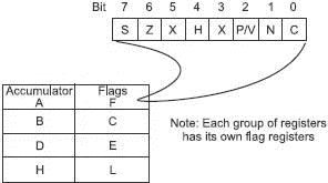
Figure 8.3 The Z80180 flag register
A note: In microprocessors, computers and electronics generally, something that is marked with an X is not used, and so we don’t care what the voltage or binary value is.
Another note: a flag is said to be ‘set’ when its value is 1 and is ‘cleared’ to 0.
Sign flag (S)
The S flag is just a copy of the bit 7 of the accumulator. A negative number has a 1 in bit 7 and a positive number has a 0 in bit 7 so this flag indicates the sign of the number. You may remember that signed magnitude numbers use a 1 to indicate a negative number and 0 to indicate a positive number. Likewise a negative number expressed in two’s complement form will have its left-hand bit as a 1. The number zero is treated as a positive number so we cannot use the S flag to spot a zero result. We do this by employing a special ‘zero’ flag as we will see in a moment.
Zero flag (Z)
The Z flag spends all its time watching for a result of zero.
You may remember that when we were looking at the uses of an XOR gate, we used this gate to check the code number in a cash dispenser. When the entered value and the card number were the same, it allowed cash to be withdrawn. What actually happened was that the two numbers were compared and if they were the same, then the result would be zero and the Z flag would spring into action. It ‘sets’ or changes to a binary 1 if it sees a zero result and stays at binary 0 at all other times.
Two things to be careful about. The Z flag only goes to a one state if all bits in the latest result are zero. Also, be careful about the way round: result 0 makes the Z flag = 1; result not zero, Z flag = 0.
All these results would give a Z flag value of zero:
0100 0000
1111 1111
0000 0001
1001 1010
Only a result of 0000 0000 would make the Z flag go to a binary 1.
Add/subtract flag (N)
The N flag is just there to tell us whether the last arithmetic instruction was ‘add’ or ‘subtract’. N=0 for add, N=1 for subtract. Not very exciting.
Carry flag (C) and the half-carry flag (H)
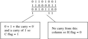
When addition is carried out, it sometimes results in a bit being carried over to the next column. The C flag copies the value of the carry from bit 7 and the H flag records the carry from bit 3 into bit 4 during additions. It also reflects the value of the ‘borrow’ in subtractions.
Here is an example of an addition showing the C and H flags.
Parity/overflow flag (P/V)
This is used for two separate purposes.
The ‘V’ in the title refers to oVerflow in arithmetic calculations. Some combinations of numbers can be misinterpreted and give an apparently incorrect answer, as we will see.
When the flag spots a possible error it is set, when no error is likely, it is cleared.
Here is an example where we could see a problem.
We are going to add two positive numbers +96 and +66 so even if we can’t guess the result, we do at least know that it is a positive number.
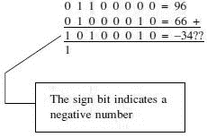
In this example, we have added two numbers that start with zero and are therefore positive and the result starts with a one, which is a negative number so the P/V flag will be set.
An easy way to check for a possible error is to look at the carry into bit 7 and the carry out of bit 7.
The rule is:

In our example, there was a 1 carried into bit 7 from the previous column but there was no bit carried out from bit 7. This does not fit into the rule above so the P/V flag will be set to 1 indicating a possible error in the result.
Its second purpose is to operate in its parity mode.
In this mode, it checks a byte of data and counts the number of 1 states, if the total is an even number, the P/V flag is set and if odd, it is cleared.
So the byte 10110101 would mean P/V=0 since the number 1 occurs 5 times, which is an odd number. And 10010110 would result in P/V=1 because there are four occasions when the number 1 occurs and 4 is an even number.
This flag operates in the P or V mode depending on the instruction being carried out at the time.
We will look at parity in more detail in Chapter 17.
The general-purpose registers
The general-purpose registers are all 8-bit registers but if we like, we can use them two at a time as 16-bit registers. When pairing them up, our choice is restricted to the way suggested by Figure 8.2. We can combine BC, DE or HL but it’s not a free choice, we cannot choose any two such as B and L. We can use a pair like BC as a 16-bit register and, at the same time, use D/E/H/L as separate 8-bit registers. As usual, the alternate register set behaves in exactly the same manner.
They have labelled the first four as B, C, D and E, so it may seem a little odd to use H and L for the last two.
The reason for this is that these registers are also used to keep track of memory addresses. The Z8018X has a 16-bit address bus and so requires a 16-bit register to be able to store a full address. The H and L stand for High and Low bytes of the address so if we wanted to store the address 2684H, we would put 84 in the L register and 26 in the H register, using binary of course. As well as being used to hold an address, the H and L registers can still be used for any other purpose that we want, just like B,C, D and E.
Special-purpose registers
Program counter (PC)
A program is a list of instructions for the microprocessor to carry out. Before use, they must be stored in some ROM or RAM. Let’s assume that we used addresses starting from 6400H. To run the program we must tell the microprocessor to ‘go’ from 6400H. What we are actually doing is loading the address 6400H into the program counter and the microprocessor starts from there. Once it has completed the instruction in 6400H, it goes to the next address 6401H and then 6402H etc until it reaches the end of the program. The purpose of the program counter is to keep track of the address that is going to be used next.
Stack pointer (SP)
If someone gave us a telephone number to remember, we would be likely to reach for a scrap of paper and a pencil to write it down. Our note may look like Figure 8.4.
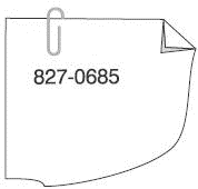
Figure 8.4 A number to remember
If we were then given another couple of numbers, we are likely to jot them down, in order, under the first one as in Figure 8.5.
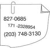
Figure 8.5 A few more numbers
We could read them back in order by reading the bottom one first, then the next and finally the top one. The first one to be entered was the last one to come out.
The microprocessor could do something similar by storing information in a series of 16-bit memory locations called a ‘stack’. The stack is loaded in order and then unloaded starting from the last number stored and working back to the top of the stack. The first number that was stored would be retrieved last and for this reason it would be called a ‘first-in, last-out’ method or FILO. For maximum confusion, this can also be called a LIFO system that, of course, means exactly the same. Have a think about it.
Inside the microprocessor, a series of RAM locations are reserved to be used as a stack and an address counter must be employed to keep track of what address of the stack is to be used next. This counter is called a stack pointer since it ‘points at’ the next address to be used.
The stack is generally used by the microprocessor to store data on a very temporary basis. We are allowed to use it but the microprocessor takes priority and doesn’t know that we have been fiddling with it. For example, if the microprocessor had stored three bits of data in order as in Figure 8.6(a) and we put one piece of our data on the end as in Figure 8.6(b), there would now be data in four locations. However, the microprocessor would not be aware of this. When the microprocessor wished to retrieve its data, it would unload three bytes and accidentally get the wrong one as in Figure 8.6(c).
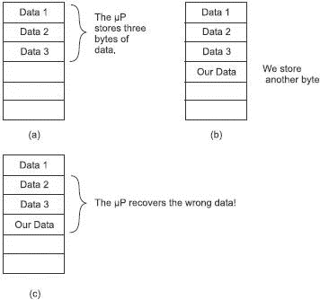
Figure 8.6 Using the stack
The moral of this story is leave the stack alone – or be very careful! The technical data will always give you sufficient information to be able to know whether or not the microprocessor will be using the stack but it still takes a lot of working through to be sure.
Index registers
We have two index registers, one called X and the other called Y. They both perform the same function.
An index is used in situations in which we wish to perform a sequence of similar tasks one after the other. Perhaps to use data stored in a series of memory locations. The 16-bit content of the index register can be added to the contents of the program counter (PC) to produce a new address.
As an example, let’s assume that we are running a program which after using address 2600H we would like it to use some data stored in address 3800H. We could do this by loading the 16-bit number 1200H into the X register and instruct the microprocessor to go to the address written as PC+IX (program counter and index X). In this case, the microprocessor goes to address 2600H+1200H=3800H to retrieve the data to be used. This jump from 2600H to 3800H is called an offset or we may say that the index X register has provided an offset of 1200H. In this example, index register Y could have been used equally well.
Index registers are often used to input data previously entered into a table or from another part of the memory. The user of a program may be asked to type in a number. This number would be entered in RAM but the program that is going to use this data is stored in ROM. A suitable offset in one of the index registers could shift the address sufficiently to bring it into the RAM area of the memory map. These registers are also used in situations where the program seeks a response from the user. The screen may show:
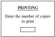
We could implement this by storing the response in one of the index registers and, as the printer performs each copy, the number stored is decreased by one (decremented) until it reaches zero. Every time that the counter is decremented, we instruct the microprocessor to check the state of the Z flag. When the count finally reaches zero, the Z flag will be set and the printer can be stopped.
R counter (R)
This is a simple counter in which the lower seven bits are used to count the number of instructions that have been carried out by the microprocessor while it has been running the present program. It is reset to zero whenever the micro is restarted.
Figure 8.7 shows the remaining parts of a microprocessor. All these parts are inside the single block marked ‘microprocessor’ (µP) in Figure 7.4. These include all the facilities for connecting the device to external circuits and a few other essentials.
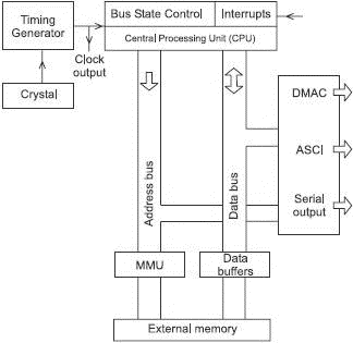
Figure 8.7 The Z80180 microprocessor
Data buffers
The data buffer is an 8-bit register to store the information being provided by the external data bus. Once the buffer stores the binary information then tri-state buffers can lock-in the information disconnecting the external data bus so it can be used for carrying other data. This process is called ‘latching’. As a general rule, all inputs to a chip from a bus are latched in. This is because the buses take time to set up new voltages on their lines and need to get started on this job as soon as possible.
The address and data buses
As with all microprocessors, there are three buses, the address, data and control. As we saw in the previous chapter, the control bus is a loose collection of connections that send signals around the system to make connections and control the operation of each area as necessary. Here we will concentrate on the address and data buses in the Z80180.
The Z80180 has a (sort of)16-bit address bus and an 8-bit data bus.
In the smaller microprocessors, it was usual practice to make the address bus twice the width of the data bus but there is no reason why this has to be the case. The choice of address bus width will depend on the anticipated size of the memory that needs to be addressed in the final designs. Unusually, in this microprocessor there are two conflicting requirements: it has to remain compatible with the 16-bit address bus of the Z80 but we would like to be able to address 1 MB which requires 20 address lines.
These requirements are met by the block shown as MMU or memory management unit.
Memory management unit (MMU)
This circuit includes an 8-bit register that holds address information that can be controlled by the software being used. These 8 bits are combined with the top four address lines, A12–A15, of the address bus. The lower half of these 8 bits are added to the top 4 bits of the address bus and the upper 4 bits are used to expand the useable memory by adding the four extra address lines, A16–A19, to allow a total of twenty lines to be addressed – see note below. The process is shown in Figure 8.8.
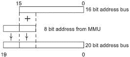
Figure 8.8 Expanding the address bus
The Z80180 family is manufactured in three different packages. The original 40 pins of the old Z80 has increased to 64 pins in the dual-inline (d.i.l.) package similar to that shown at the top of Figure 1.6. They also make a 68 pin plastic leaded chip carrier (PLCC) version which is just like the square package in Figure 1.6. Finally, there is an 80 pin surface mount type.
Surface mount devices do not have pins that go through holes in the printed circuit board but have connectors that come out horizontally and then soldered onto the surface of the board. This method allows significant space savings.
- 4.4.4 The Dispatcher
- About the author
- Chapter 7. The state machine
- Appendix E. Other resources and links
- Example NAT machine in theory
- The final stage of our NAT machine
- Compiling the user-land applications
- The conntrack entries
- Untracked connections and the raw table
- Basics of the iptables command
- Other debugging tools
- Setting up user specified chains in the filter table
