Книга: Introduction to Microprocessors and Microcontrollers
A serious piece of test equipment
A serious piece of test equipment
All the previous pieces of test gear have failed when we try to see what is happening on the address and data buses under real operating conditions. The oscilloscope cannot watch more than two different places at the same time but we may need to monitor a larger number, perhaps 50 or more places and then slowly check the information back or print it out. An instrument called a logic analyser can achieve all these functions and much more.
It can answer such questions as:
• What values actually appear on the address bus when we cause an interrupt to occur?
• Is the correct program actually being run?
• Are there any unwanted voltage spikes occurring?
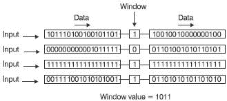
The design of a logic analyser is basically a very simple combination of shift registers. You may remember we looked at shift registers in Chapter 6. The register was loaded with data and, on each clock pulse, the data is moved one place to the left or right as required. Now imagine a shift-right register that can hold 36 bits of data. If we connect it to A0, the first line of the address bus, and run a program, the logic values of that address line will be copied onto the shift register, pass along to the end with each clock pulse and eventually start to fall out the far end (see Figure 18.7).

Figure 18.7
Now if we had four such registers, we could collect data from any four parts of a circuit at the same time. For example, we could monitor the lowest four address lines, which would be called A0, A1, A2 and A3.
In the centre of the register is a window. This means that we can access the centre of the shift register at this point to read off the data and to make comparisons. In Figure 18.8 only the four registers are shown for clarity. A simple arrangement like this would be referred to as a 4?16 (four by sixteen) logic analyser. In logic analyser specifications, the number of registers would be spoken of as the number of channels. In real life, we would never find such a simple arrangement of registers. Logic analysers could contain, say, 80 channels, each containing 4096-bit shift registers. This would be referred to as a 80?4 kbyte logic analyser. With one this size, we could monitor any 80 different points on a microprocessor-based system. Which points we choose are up to us, we could choose the whole of the address bus and the data bus and some control signals or any other points of interest. The choice is entirely ours.
If, in Figure 18.8, the four registers were being used to monitor four address lines, we may be suspicious of the line showing a constant value of logic 1. This may indicate that this line has become short-circuited to a positive power supply, or be disconnected and is floating high. Don’t leap off your chair in excitement though – this is only one explanation. It could happen for these reasons or it could be running a part of the program where this would be the expected result.

Figure 18.8 Four shift registers can make a simple logic analyser
So what about the window?
In the window, the logic analyser will ‘see’ a bit of data from each of the channels. We can load the combination that we are searching for. For convenience, we enter the values in hex numbers and as the clock pulses arrive from the microprocessor, the data moves across and is continuously compared with the number we have entered. When a match is found, the clock is switched off and the data is ‘captured’. We can now move backwards and forwards along the registers and see the operation of the microprocessor ‘frozen’ in time. The benefit of positioning the window in the centre of the shift register is that it allows us to observe the program action before, as well as after, the chosen moment.
Extra facilities
A ‘real’ logic analyser has some extra facilities, like performing the capture not on the first time our input is seen but after perhaps the 200th occasion to take care of repetitive loops in the program. They also allow a ‘don’t care’ condition on the inputs so in the window of a 20-channel logic analyser we could enter the hex code 7XXX2. This would perform a capture on any data that starts with 7H (01112) and ends with 2H (00102).
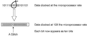
A glitch is a very short duration pulse that can occur in logic circuits, either from external interference or as a result of poor design. They can cause unwanted switching in the logic circuit and cause the microprocessor program to crash. They are exceedingly short, just a few nanoseconds and this makes spotting them very difficult. They are usually too fast for an oscilloscope but some logic probes have a ‘glitch-catcher’ built in, but they can only tell us that a glitch has occurred, not when it occurred. This is the information that will be needed if we are to track down a design problem.
A logic analyser may miss it because the incoming data is sampled once per pulse and if it misses the glitch it will not be recorded. To overcome this, the logic analyser can use its own internal clock that is running much faster than the system clock so a single logic one may extend for 10 or 20 bits in the register and a glitch may well be recorded. Figure 18.9 shows the internal clock running at 10 times the microprocessor clock. Some logic analysers have a built-in glitch catcher and use it to capture the correct section of data. As we can see, the logic analyser is a very useful and sophisticated piece of kit. Using it, however, is a slow process. There are lots of connections to be made to the circuit and much sitting and thinking.

Figure 18.9 Glitch catching
- Simple test equipment
- 18. Test equipment and fault-finding
- rc.test-iptables.txt
- Example rc.test-iptables script
- Testing the Project
- Testing Wdm2 Power Capabilities
- Test Driver Code
- Тестовые данные (Test Data)
- Testing Samba with the testparm Command
- Creating a File System for Testing
- Testing the Program
- Testing the Project


