Книга: Introduction to Microprocessors and Microcontrollers
The Pentium 4
The Pentium 4
As we have mentioned before, one of the limits on operational speed is the size of the internal components and, until recently the smallest detail was limited to 0.18 µm. As the competition between the AMD continued, it was time for the next step as AMD started using 0.13 µm technology and, as expected, the Pentium 4 also upgraded to the same technology for the faster versions of 1.8 GHz and above. The operating voltage has also been reduced from 1.75 down to 1.5 volts allowing closer spacing and a further increase in speed (and 25% reduction in cost). The new design has allowed the Pentium 4 to increase its transistor headcount from 42 million to 55 million increasing the number of connecting pins to 478. Intel has moved a long way from the 16 pins of their 4-bit offering in 1972.
Thermal safety
The power dissipation increases as any integrated circuit works faster and the Pentium 4 is no exception. Now, bearing in mind that the actual processor circuit is just 10 mm?10 mm (0.4 square inches) and consumes 55 watts. We must be very careful to ensure that it doesn’t overheat. This is achieved by using a large heat sink and a cooling fan. The new Pentium has a thermal safety circuit. If the microprocessor starts to overheat, the cooling fan will increase its revs and the operating speed of the microprocessor will decrease. If things get serious and it reaches a dangerous level of 69°C (155°F) the thermal circuit will call it a day and shut down the computer to prevent the microprocessor from being destroyed.
The system bus
Also called the FSB or Front Side Bus, is 64 bits wide and ‘Quad Pumped’ which is a fancy way of saying that each clock pulse, presently running at 133 MHz, will shift four lots of data along the bus. Now, rounding off the figures a bit, 133 MHz?4=533 MHz so the bus looks like a single 533 MHz bus. Incoming and outgoing information is stored in the 256 kB level 2 Advanced Transfer Cache which is fed 256 bit wide pathways. Intel calls it ‘Advanced Transfer Cache’ which is not quad pumped though being wider, still matches the speed of the system bus.
Instruction Decoder, Level 1 Execution Trace Cache and Branch Predictor
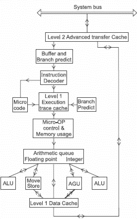
The data that is selected by the predictor is loaded into a buffer and then passed onto the Instruction Decoder.
At this stage, the incoming instructions are analysed and converted into an internal code sequence which can be accessed from the Micro code as we saw when we looked at the Z80180 microprocessor. Once the instructions have been decoded, up to about 12 000
instructions called ‘Micro-Operation/Operand’ or µOP are stored in order of use, all ready to go. The correct order is much assisted by the Branch prediction – known by Intel as the Branch Target Buffer (BTB). This stores previous experience to guess what is likely to happen next.
Hyper pipeline
As we saw in Chapter 11, the pipeline is the organization of the microprocessor and not a separate device within the design, so we don’t get a ‘pipeline’ block shown in Figure 12.3. The predictor designs are now very much improved, having had the experience gained with earlier versions of the Pentium. The better the prediction, the longer and faster we can risk make the pipeline. So pleased were Intel with their predictions that they called the new longer pipeline a ‘hyper pipeline’. For maximum speed we would like a long pipeline so that many simple steps can be carried out at greater speed but the overall outcome depends on the predictor circuits making the right guess. A wrong guess means that the pipeline is loaded with incorrect data and has to be refilled, or ‘flushed’, which takes valuable time. The Pentium 4 now has a pipeline of 20 stages which allow 126 instructions to be in use at a single time which can include up to 48 load and 24 store instructions.

Figure 12.3 The Pentium 4 processor
Micro-OP and Memory usage
The µOps that pour out of the Execution Trace Cache are arranged in order and they will be a mixture of information to be stored in memory locations and arithmetic operations. The arithmetic operations are divided in floating-point operations and integer operations. The floating-point register deals with moving and storing while the ALU (Arithmetic and Logic Unit) deals with the more complex operations such as multiplication of 128-bit numbers and MMX (multimedia instructions) as we met a little earlier. The SIMD (Single Instruction Multiple Data) that was applied to the earlier Pentiums have been extended by an extra 144 instructions. This facility is now called SSE2 (Streaming SIMD Extensions 2 instructions). The general idea is that if we have to perform an action on many bits of data, it is simpler and faster to collect them all together and perform the function on all of them at the same time.
Rapid Execution Engine
For the integer instructions there are two ALUs clocked at twice the core processor speed which is a four-fold improvement over the basic function and provides a data transfer rate of 48 GB/s.
A level 1 data cache handles the data outputs from the ALUs and the AGUs (Address Generation Units).


