Книга: Introduction to Microprocessors and Microcontrollers
The PowerPC 601 (or MPC601)
The PowerPC 601 (or MPC601)
The PowerPC 601 was introduced in 1994 and followed the agreed PowerPC architecture as shown in Figure 13.1. It used 2.8 million transistors which is slightly less than the Pentium but many of the Pentium transistors were tied up with maintaining compatibility with their earlier microprocessors.
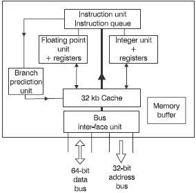
Figure 13.1 The PowerPC 601 architecture
Many of the blocks shown are familiar after our look at the Pentium. The 601 is a 32-bit microprocessor using a 64-bit data bus and a 32-bit address bus.
Bus interface unit
This serves the usual purpose of connecting the data bus and address buses to the microprocessor. It also acts as a control device to determine whether the data is to be read into the microprocessor or written into the external memory.
Cache
This is a single 32 kbyte cache which is shared by data and instructions. Later versions have increased the total cache available to provide two separate 32 kbyte caches, one for data and the other for instructions.
Within the cache, the information is arranged in a series of groups or lines of 64 bytes. To provide a high-speed link between the cache, the bus interface unit and the instruction unit and queue, a 256-bit internal bus is provided.
On many occasions, the result of a particular instruction is not of great interest in itself but just provides the data to be used for a future instruction. So when an instruction is completed, the result is stored in the cache rather than being put back into the main memory. Writing the result back into the cache is called a ‘write-back’ organization as opposed to ‘write-through’ action when the information is sent to the external memory. This, of course, saves a lot of time since the cache is about seven times faster than accessing the main memory and a million times faster than using the hard drive.
Instruction queue and instruction unit
The fast internal bus maintains a queue of up to eight instructions. Using the normal RISC ideas, all the instructions are the same length at 32 bits. Eight such instructions can fit across the 256-bit width of the internal bus.
The function of the instruction unit is to send instructions to the three pipelines: integer unit, floating-point unit and the branch prediction unit. With the right mixture of instructions, we can handle three instructions at the same time. To keep the pipelines busy, it also has the facility of running some of the instruction out of order. This is limited to instructions that are not interdependent.
The branch prediction unit
In the Pentium, the branch prediction included analysis of the history of each branch or jump instruction to help predict whether it is likely to be taken. The PowerPC uses a single stage pipeline which decodes and executes in a single clock cycle employing a very much simpler strategy that curiously seems to work just as well.
It makes no choices. If the branch is sending the program back to an earlier instruction, it always assumes that the branch will be taken. This is usually the correct choice since such loops in programs are very common. On the other hand, if the branch instruction offers the chance to jump forward, it assumes the branch will not be taken. If the predictions are correct, instructions are pre-fetched and loaded into the instruction queue and the correct data is available in the pipelines and no delay is experienced. If incorrect, the pipeline has to be flushed and reloaded losing several clock cycles.
In the case of unconditional jumps, the program just tells the microprocessor to move to another section of the program and no choice is involved. If the jump is to a distant address, the relevant instructions may not be in the cache and the cache would have to be flushed (re-loaded) (see Figure 13.2).
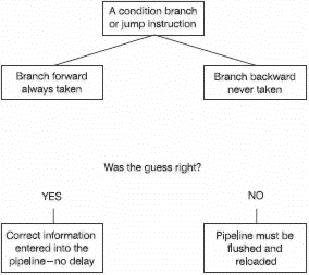
Figure 13.2 Branch prediction
Integer unit and registers
As expected with a RISC processor, there are plenty of registers. In this section of the 601, we have 32 registers, each 32-bits wide. These registers are dual-ported. This means that two circuits can access the registers at the same time without interfering with each other. This is like someone reading the back of your newspaper as you are reading the front – except that registers don’t find it irritating. ‘Port’, by the way, is just a fancy electronic word meaning ‘connection’. Transistors, generally, have three wires going to them and so are described as three-port devices.
The integer unit handles all instructions like integer arithmetic bit manipulation and transferring data to and from the external memory and is organized into a three-stage pipeline. In Figure 13.3, the second clock pulse executes the first instruction. The next clock pulse executes the second instruction and the last clock pulse executes the third. We have achieved the target of one clock pulse per clock pulse. And in the fourth clock pulse, we can see the next instruction just arriving to be decoded immediately after the first write-back.
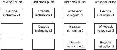
Figure 13.3 Integer unit pipeline
Floating-point unit
This has a further 32 registers but in this case, they are 64-bits wide and to fill a register with a single clock pulse, there is an internal 64-bit bus connecting it with the cache. The pipeline is five stage: prefetch, buffer, decode, execution and write-back.
Memory buffer
This acts as a buffer for the external memory. The buffers include two reads and three writes, each up to 32 bytes. It is also used in writing-back to the cache.
Big and little endians
The main memory is divided into locations each having its own address. Each location can hold a single byte of information. If we wanted to store a 32-bit number, then we would have to utilize four consecutive locations.
Imagine that we wished to store the 32-bit number 00000000 01010101 00010001 111111112 and we had addresses 24646603H, 24646602H, 24646601H and 24646600H available. Little-endian format would store the most significant byte in the highest memory address so, in our example, the data 00000000 would go into address 24646603H. This is used by Intel microprocessors. Big-endian, which Motorola uses, works the other way around. The most significant byte is put in the lowest memory address so, in our example, the data 00000000 would go into address 24646600H. These are shown in Figure 13.4. All the PowerPC microprocessors are switchable to enable little or big-endian to be used.
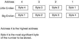
Figure 13.4 Big and little endians
- 3.2.3. Freescale PowerPC
- 4.4.4 The Dispatcher
- About the author
- Chapter 7. The state machine
- Appendix E. Other resources and links
- Example NAT machine in theory
- The final stage of our NAT machine
- Compiling the user-land applications
- The conntrack entries
- Untracked connections and the raw table
- Basics of the iptables command
- Other debugging tools
