Книга: Introduction to Microprocessors and Microcontrollers
Another look at the address decoder
Another look at the address decoder
We have seen in Chapter 6 that the number of locations that can be addressed is 2nwhere n is the number of address lines. By feeding the numbers into our calculators we can see that the relationship between lines and locations is as shown in Table 7.1.
Table 7.1 Larger memories need more address lines
| Number of address lines | Number of locations | Number of address lines | Number of locations | Number of address lines | Number of locations |
|---|---|---|---|---|---|
| 1 | 2 | 13 | 8k | 25 | 32M |
| 2 | 4 | 14 | 16k | 26 | 64M |
| 3 | 8 | 15 | 32k | 27 | 128M |
| 4 | 16 | 16 | 64k | 28 | 256M |
| 5 | 32 | 17 | 128k | 29 | 512M |
| 6 | 64 | 18 | 256k | 30 | 1024M=1G |
| 7 | 128 | 19 | 512k | 31 | 2G |
| 8 | 256 | 20 | 1024k=1M | 32 | 4G |
| 9 | 512 | 21 | 2M | 33 | 8G |
| 10 | 1024 = 1k | 22 | 4M | 34 | 16G |
| 11 | 2k | 23 | 8M | 35 | 32G |
| 12 | 4k | 24 | 16M | 36 | 64G |
We can also use this table to identify the number of lines needed to access a known number of address locations. For example, if we wanted to access 700 locations, we can see that 9 lines could access 512 locations which is too few. Therefore, we would have to go to 10 lines which would actually give access to 1024 locations. The ‘real’ answer of 9.45 is not sensible because we cannot have 0.45 of a connecting wire so if 9 is not enough, it will have to be 10. For those who like to see the calculations, the mathematical result is given by:

Designing a decoding circuit
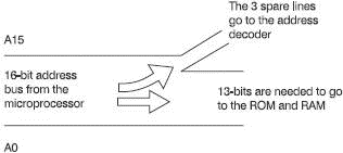
Let’s imagine that we have a microprocessor-based system using eight memory chips, ROM or RAM it doesn’t matter. Each of the chips holds 8 kbytes of memory. From Table 7.1 we can see that an 8 kbytes chip will require 13 address lines in order to access each of their internal locations. Assume too, that the microprocessor that we are using has a 16-bit address bus so we have the situation shown in Figure 7.7. The address lines are numbered from A0 (address line number 0) to A15. The 13 bits A0–A12 are heading off towards the ROM and RAM chips. The remaining three address lines, A13–A15, are used by the address decoder.

Figure 7.7 There are three ‘spare’ address lines
The decoding chip
The decoder circuit can be made from separate logic gates or can be bought ready-built in a single integrated circuit. For ease of construction, most designers opt for this choice for the result is smaller, dissipates less heat and is less expensive (and it works first time). There is very little to be said for the build-it-yourself approach.
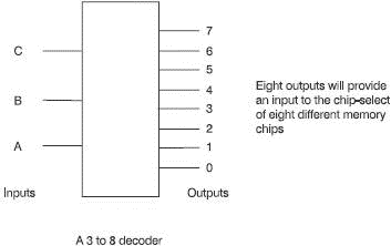
The basic requirements are three input address lines and eight output lines each connected to one of the chip select pins on a memory chip.
To switch the chips on, the chip select must be taken to a logic 0 voltage. A logic 1 voltage level will switch the chip off. It is vital, of course, that only one chip can be switched on at the same time otherwise they will load competing data onto the data bus and are likely to be destroyed. The three addresses can result in 2?=8 different inputs to the logic gates built into the decoder chip. The internal design ensures that when the address pins are all at zero, the first output goes to a logic 0 and all the others remain high. The memory chip to which this first output is connected is switched on and all the others are on. When the next combination of inputs 0, 0, 1 is applied, the second memory chip is switched on and the others are off. The next combination switches on the next memory chip and so on until the three input wires have switched on each of the memory chips with a single combination of addresses (see Figure 7.8). With three inputs and eight outputs, it is referred to, reasonably enough, as a 3 to 8 decoder.

Figure 7.8 The operation of the address decoder
Table 7.2 looks a lot worse than it really is. It is really just a summary of the decoder chip outputs. If the microprocessor put the address C2F1H on the address bus, then in binary it would be: 1100 0010 1111 0001. It has been broken up into groups of four Table 7.2 The 3–8 decoder can control eight memory chips just to make it a little easier to read. The most significant bit, A15, is on the left-hand end.
Table 7.2 The 3–8 decoder can control eight memory chips
| Inputs | Outputs | Results | |||||||||
|---|---|---|---|---|---|---|---|---|---|---|---|
| C | B | A | 0 | 1 | 2 | 3 | 4 | 5 | 6 | 7 | |
| 0 | 0 | 0 | 0 | 1 | 1 | 1 | 1 | 1 | 1 | 1 | Chip 0 selected |
| 0 | 0 | 1 | 1 | 0 | 1 | 1 | 1 | 1 | 1 | 1 | Chip 1 selected |
| 0 | 1 | 0 | 1 | 1 | 0 | 1 | 1 | 1 | 1 | 1 | Chip 2 selected |
| 0 | 1 | 1 | 1 | 1 | 1 | 0 | 1 | 1 | 1 | 1 | Chip 3 selected |
| 1 | 0 | 0 | 1 | 1 | 1 | 1 | 0 | 1 | 1 | 1 | Chip 4 selected |
| 1 | 0 | 1 | 1 | 1 | 1 | 1 | 1 | 0 | 1 | 1 | Chip 5 selected |
| 1 | 1 | 0 | 1 | 1 | 1 | 1 | 1 | 1 | 0 | 1 | Chip 6 selected |
| 1 | 1 | 1 | 1 | 1 | 1 | 1 | 1 | 1 | 1 | 0 | Chip 7 selected |
In Table 7.3, we can see that 13 out of the 16 address lines go to the memory chip and the other three are fed to the decoder chip. The three lines going to the decoder chip carry the data 1 1 0. We can see that the values C=1, B=1 and A=0 occur near the bottom of the table. These values result in Chip 6 receiving a logic 0 value and thus being selected for use. All other chips are deselected by the logic 1.
Table 7.3 In full decoding, every address line is used A
| A15 | A14 | A13 | A12 | A11 | A10 | A9 | A8 | A7 | A6 | A5 | A4 | A3 | A2 | A1 | A0 |
|---|---|---|---|---|---|---|---|---|---|---|---|---|---|---|---|
| 1 | 1 | 0 | 0 | 0 | 0 | 1 | 0 | 1 | 1 | 1 | 1 | 0 | 0 | 0 | 1 |
| ?This selects chip 6? | ?This address is internally declared within the memory chip and points to single memory location? | ||||||||||||||
- 4.4.4 The Dispatcher
- About the author
- Chapter 7. The state machine
- Appendix E. Other resources and links
- Example NAT machine in theory
- The final stage of our NAT machine
- Compiling the user-land applications
- The conntrack entries
- Untracked connections and the raw table
- Basics of the iptables command
- Other debugging tools
- Setting up user specified chains in the filter table


