Книга: Embedded Linux Primer: A Practical, Real-World Approach
2.3.1. Flash Memory
2.3.1. Flash Memory
Nearly everyone is familiar with CompactFlash modules[5] used in a wide variety of consumer devices, such as digital cameras and PDAs (both great examples of embedded systems). These modules can be thought of as solid-state hard drives, capable of storing many megabytesand even gigabytesof data in a tiny footprint. They contain no moving parts, are relatively rugged, and operate on a single common power supply voltage.
Several manufacturers of Flash memory exist. Flash memory comes in a variety of physical packages and capacities. It is not uncommon to see embedded systems with as little as 1MB or 2MB of nonvolatile storage. More typical storage requirements for embedded Linux systems range from 4MB to 256MB or more. An increasing number of embedded Linux systems have nonvolatile storage into the gigabyte range.
Flash memory can be written to and erased under software control. Although hard drive technology remains the fastest writable media, Flash writing and erasing speeds have improved considerably over the course of time, though flash write and erase time is still considerably slower. Some fundamental differences exist between hard drive and Flash memory technology that you must understand to properly use the technology.
Flash memory is divided into relatively large erasable units, referred to as erase blocks. One of the defining characteristics of Flash memory is the way in which data in Flash is written and erased. In a typical Flash memory chip, data can be changed from a binary 1 to a binary 0 under software control, 1 bit/word at a time, but to change a bit from a zero back to a one, an entire block must be erased. Blocks are often called erase blocks for this reason.
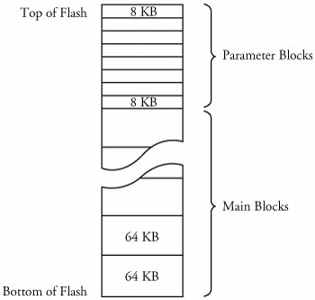
A typical Flash memory device contains many erase blocks. For example, a 4MB Flash chip might contain 64 erase blocks of 64KB each. Flash memory is also available with nonuniform erase block sizes, to facilitate flexible data-storage layout. These are commonly referred to as boot block or boot sector Flash chips. Often the bootloader is stored in the smaller blocks, and the kernel and other required data are stored in the larger blocks. Figure 2-3 illustrates the block size layout for a typical top boot Flash.
Figure 2-3. Boot block flash architecture

To modify data stored in a Flash memory array, the block in which the modified data resides must be completely erased. Even if only 1 byte in a block needs to be changed, the entire block must be erased and rewritten.[6] Flash block sizes are relatively large, compared to traditional hard-drive sector sizes. In comparison, a typical high-performance hard drive has writable sectors of 512 or 1024 bytes. The ramifications of this might be obvious: Write times for updating data in Flash memory can be many times that of a hard drive, due in part to the relatively large quantity of data that must be written back to the Flash for each update. These write cycles can take several seconds, in the worst case.
Another limitation of Flash memory that must be considered is Flash memory cell write lifetime. A Flash memory cell has a limited number of write cycles before failure. Although the number of cycles is fairly large (100K cycles typical per block), it is easy to imagine a poorly designed Flash storage algorithm (or even a bug) that can quickly destroy Flash devices. It goes without saying that you should avoid configuring your system loggers to output to a Flash-based device.
- 2.3.2. NAND Flash
- 2.3.3. Flash Usage
- 2.3.4. Flash File Systems
- 2.3.5. Memory Space
- 2.3.7. Process Virtual Memory
- Flash Memory Support
- EVENT MEMORY SIZE
- Flash-накопители
- В Интернете можно найти большое количество игр, баннеров и меню, сделанных во Flash. Можно ли самому создать подобную ан...
- Переносные устройства на основе flash-памяти
- 12.2.1 Port-Mapped vs. Memory-Mapped I
- Displaying Free and Used Memory with free


