Книга: Advanced PIC Microcontroller Projects in C
2.1.11 Analog-to-Digital Converter (A/D) Module
2.1.11 Analog-to-Digital Converter (A/D) Module
An analog-to-digital converter (A/D) is another important peripheral component of a microcontroller. The A/D converts an analog input voltage into a digital number so it can be processed by a microcontroller or any other digital system. There are many analog-to-digital converter chips available on the market, and an embedded systems designer should understand the characteristics of such chips so they can be used efficiently.
As far as the input and output voltage are concerned A/D converters can be classified as either unipolar and bipolar. Unipolar A/D converters accept unipolar input voltages in the range 0 to +0V, and bipolar A/D converters accept bipolar input voltages in the range ±V. Bipolar converters are frequently used in signal processing applications, where the signals by nature are bipolar. Unipolar converters are usually cheaper, and they are used in many control and instrumentation applications.
Figure 2.40 shows the typical steps involved in reading and converting an analog signal into digital form, a process also known as signal conditioning. Signals received from sensors usually need to be processed before being fed to an A/D converter. This processing usually begins with scaling the signal to the correct value. Unwanted signal components are then removed by filtering the signal using classical filters (e.g., a low-pass filter). Finally, before feeding the signal to an A/D converter, the signal is passed through a sample-and-hold device. This is particularly important with fast real-time signals whose value may be changing between the sampling instants. A sample-and-hold device ensures that the signal stays at a constant value during the actual conversion process. Many applications required more than one A/D, which normally involves using an analog multiplexer at the input of the A/D. The multiplexer selects only one signal at any time and presents this signal to the A/D converter. An A/D converter usually has a single analog input and a digital parallel output. The conversion process is as follows:
• Apply the processed signal to the A/D input
• Start the conversion
• Wait until conversion is complete
• Read the converted digital data
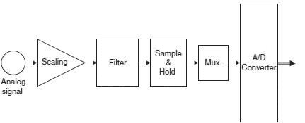
Figure 2.40: Signal conditioning and A/D conversion process
The A/D conversion starts by triggering the converter. Depending on the speed of the converter, the conversion process itself can take several microseconds. At the end of the conversion, the converter either raises a flag or generates an interrupt to indicate that the conversion is complete. The converted parallel output data can then be read by the digital device connected to the A/D converter.
Most members of the PIC18F family contain a 10-bit A/D converter. If the chosen voltage reference is +5V, the voltage step value is:

Therefore, for example, if the input voltage is 1.0V, the converter will generate a digital output of 1.0/0.00489 = 205 decimal. Similarly, if the input voltage is 3.0V, the converter will generate 3.0/0.00489 = 613.
The A/D converter used by the PIC18F452 microcontroller has eight channels, named AN0–AN7, which are shared by the PORTA and PORTE pins. Figure 2.41 shows the block diagram of the A/D converter.
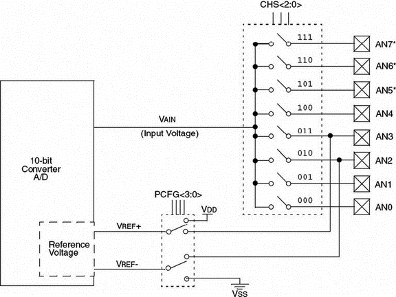
Figure 2.41: Block diagram of the PIC18F452 A/D converter
The A/D converter has four registers. Registers ADRESH and ADRESL store the higher and lower results of the conversion respectively. Register ADCON0, shown in Figure 2.42, controls the operation of the A/D module, such as selecting the conversion clock together with register ADCON1, selecting an input channel, starting a conversion, and powering up and shutting down the A/D converter.
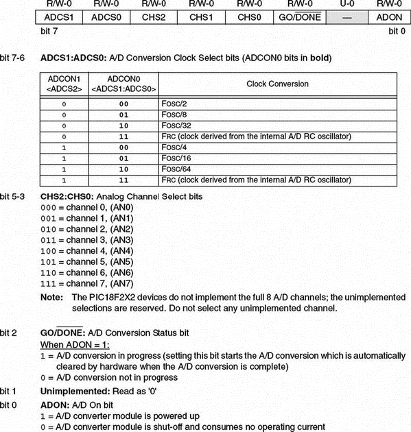
Figure 2.42: ADCON0 register
Register ADCON1 (see Figure 2.43) is used for selecting the conversion format, configuring the A/D channels for analog input, selecting the reference voltage, and selecting the conversion clock together with register ADCON0.
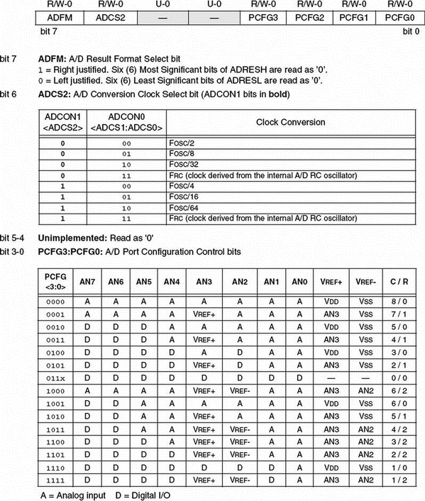
Figure 2.43: ADCON1 register
A/D conversion starts by setting the GO/DONE bit of ADCON0. When the conversion is complete, the 2 bits of the converted data is written into register ADRESH, and the remaining 8 bits are written into register ADRESL. At the same time the GO/DONE bit is cleared to indicate the end of conversion. If required, interrupts can be enabled so that a software interrupt is generated when the conversion is complete.
The steps in carrying out an A/D conversion are as follows:
• Use ADCON1 to configure required channels as analog and configure the reference voltage.
• Set the TRISA or TRISE bits so the required channel is an input port.
• Use ADCON0 to select the required analog input channel.
• Use ADCON0 and ADCON1 to select the conversion clock.
• Use ADCON0 to turn on the A/D module.
• Configure the A/D interrupt (if desired).
• Set the GO/DONE bit to start conversion.
• Wait until the GO/DONE bit is cleared, or until a conversion complete interrupt is generated.
• Read the converted data from ADRESH and ADRESL.
• Repeat these steps as required.
For correct A/D conversion, the A/D conversion clock must be selected to ensure a minimum bit conversion time of 1.6?s. Table 2.11 gives the recommended A/D clock sources for various microcontroller operating frequencies. For example, if the microcontroller is operated from a 10MHz clock, the A/D clock source should be FOSC/16 or higher (e.g., FOSC/32).
Table 2.11: A/D conversion clock selection
| A/D clock source | ||
|---|---|---|
| Operation | ADCS2:ADCS0 | Maximum microcontroller frequency |
| 2 TOSC | 000 | 1.25 MHz |
| 4 TOSC | 100 | 2.50 MHz |
| 8 TOSC | 001 | 5.0 MHz |
| 16 TOSC | 101 | 10.0 MHz |
| 32 TOSC | 010 | 20.0 MHz |
| 64 TOSC | 110 | 40.0 MHz |
| RC | 011 | – |
Bit ADFM of register ADCON1 controls the format of a conversion. When ADFM is cleared, the 10-bit result is left justified (see Figure 2.44) and lower 6 bits of ADRESL are cleared to 0. When ADFM is set to 1 the result is right justified and the upper 6 bits of ADRESH are cleared to 0. This is the mode most commonly used, in which ADRESL contains the lower 8 bits, and bits 0 and 1 of ADRESH contain the upper 2 bits of the 10-bit result.
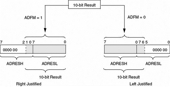
Figure 2.44: Formatting the A/D conversion result
Analog Input Model and Acquisition Time
An understanding of the A/D analog input model is necessary to interface the A/D to external devices. Figure 2.45 shows the analog input model of the A/D. The analog input voltage VAIN and the source resistance RS are shown on the left side of the diagram. It is recommended that the source resistance be no greater than 2.5K. The analog signal is applied to the pin labeled ANx. There is a small capacitance (5pF) and a leakage current to the ground of approximately 500nA. RIC is the interconnect resistance, which has a value of less than 1K. The sampling process is shown with switch SS having a resistance RSS whose value depends on the voltage as shown in the small graph at the bottom of Figure 2.45. The value of RSS is approximately 7K at 5V supply voltage.
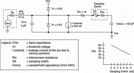
Figure 2.45: Analog input model of the A/D converter
The A/D converter is based on a switched capacitor principle, and capacitor CHOLD shown in Figure 2.45 must be charged fully before the start of a conversion. This is a 120pF capacitor which is disconnected from the input pin once the conversion is started.
The acquisition time can be calculated by using Equation (2.7), provided by Microchip Inc:
TACQ = Amplifier settling time + Holding capacitor charging time + temperature coefficient (2.7)
The amplifier settling time is specified as a fixed 2?s. The temperature coefficient, which is only applicable if the temperature is above 25°C, is specified as:
Temperature coefficient = (Temperature – 25°C)(0.05?s/°C) (2.8)
Equation (2.8) shows that the effect of the temperature is very small, creating about 0.5?s delay for every 10°C above 25°C. Thus, assuming a working environment between 25°C and 35°C, the maximum delay due to temperature will be 0.5?s, which can be ignored for most practical applications.
The holding capacitor charging time as specified by Microchip Inc is:
Holding capacitor charging time = –(120pF)(1K + RSS + RS)Ln(1/2048) (2.9)
Assuming that RSS = 7K, RS = 2.5K, Equation (2.9) gives the holding capacitor charging time as 9.6?s.
The acquisition time is then calculated as:
TACQ = 2 + 9.6 + 0.5 = 12.1?s
A full 10-bit conversion takes 12 A/D cycles, and each A/D cycle is specified at a minimum of 1.6?s. Thus, the fastest conversion time is 19.2?s. Adding this to the best possible acquisition time gives a total time to complete a conversion of 19.2+12.1=31.3?s.
When a conversion is complete, it is specified that the converter should wait for two conversion periods before starting a new conversion. This corresponds to 2?1.6=3.2?s. Adding this to the best possible conversion time of 31.3?s gives a complete conversion time of 34.5?s. Assuming the A/D converter is used successively, and ignoring the software overheads, this implies a maximum sampling frequency of about 29KHz.
- 2.1.1 Program Memory Organization
- 2.1.2 Data Memory Organization
- 2.1.3 The Configuration Registers
- 2.1.4 The Power Supply
- 2.1.5 The Reset
- 2.1.6 The Clock Sources
- 2.1.7 Watchdog Timer
- 2.1.8 Parallel I/O Ports
- 2.1.9 Timers
- 2.1.10 Capture/Compare/PWM Modules (CCP)
- 2.1.11 Analog-to-Digital Converter (A/D) Module
- 2.1.12 Interrupts
- Handheld Digital Cameras
- 1.3 Microcontroller Features
- 1.3.1 Supply Voltage
- 1.3.7 Brown-out Detector
- 1.3.8 Analog-to-Digital Converter
- 1.3.9 Serial Input-Output
- 1.3.10 EEPROM Data Memory
- 1.3.12 Analog Comparator
- 1.3.13 Real-time Clock
- 2.1.11 Analog-to-Digital Converter (A
- Using Digital Cameras with Fedora
- Использование Analog
