Книга: Advanced PIC Microcontroller Projects in C
2.1 PIC18FXX2 Architecture
As shown in Table 2.1, the PIC18FXX2 series consists of four devices. PIC18F2X2 microcontrollers are 28-pin devices, while PIC18F4X2 microcontrollers are 40-pin devices. The architectures of the two groups are almost identical except that the larger devices have more input-output ports and more A/D converter channels. In this section we shall be looking at the architecture of the PIC18F452 microcontroller in detail. The architectures of other standard PIC18F-series microcontrollers are similar, and the knowledge gained in this section should be enough to understand the operation of other PIC18F-series microcontrollers.
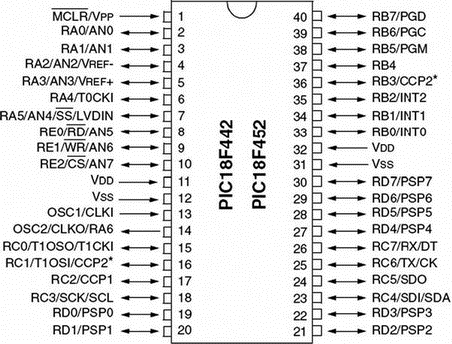
The pin configuration of the PIC18F452 microcontroller (DIP package) is shown in Figure 2.1. This is a 40-pin microcontroller housed in a DIL package, with a pin configuration similar to the popular PIC16F877.

Figure 2.1: PIC18F452 microcontroller DIP pin configuration
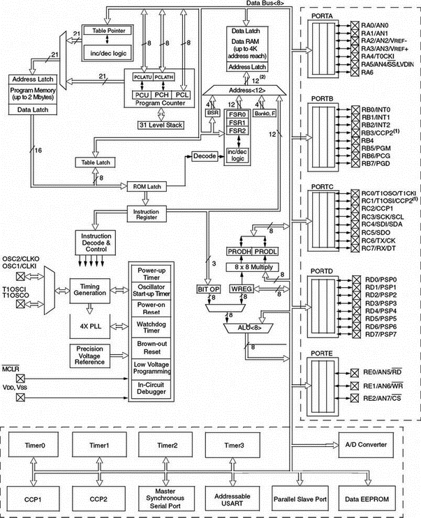
Figure 2.2 shows the internal block diagram of the PIC18F452 microcontroller. The CPU is at the center of the diagram and consists of an 8-bit ALU, an 8-bit working accumulator register (WREG), and an 8?8 hardware multiplier. The higher byte and the lower byte of a multiplication are stored in two 8-bit registers called PRODH and PRODL respectively.

Figure 2.2: Block diagram of the PIC18F452 microcontroller
The program counter and program memory are shown in the upper left portion of the diagram. Program memory addresses consist of 21 bits, capable of accessing 2Mbytes of program memory locations. The PIC18F452 has only 32Kbytes of program memory, which requires only 15 bits. The remaining 6 address bits are redundant and not used. A table pointer provides access to tables and to the data stored in program memory. The program memory contains a 31-level stack which is normally used to store the interrupt and subroutine return addresses.
The data memory can be seen at the top center of the diagram. The data memory bus is 12 bits wide, capable of accessing 4Kbytes of data memory locations. As we shall see later, the data memory consists of special function registers (SFR) and general purpose registers, all organized in banks.
The bottom portion of the diagram shows the timers/counters, capture/compare/PWM registers, USART, A/D converter, and EEPROM data memory. The PIC18F452 consists of:
• 4 timers/counters
• 2 capture/compare/PWM modules
• 2 serial communication modules
• 8 10-bit A/D converter channels
• 256 bytes EEPROM
The oscillator circuit, located at the left side of the diagram, consists of:
• Power-up timer
• Oscillator start-up timer
• Power-on reset
• Watchdog timer
• Brown-out reset
• Low-voltage programming
• In-circuit debugger
• PLL circuit
• Timing generation circuit
The PLL circuit is new to the PIC18F series and provides the option of multiplying up the oscillator frequency to speed up the overall operation. The watchdog timer can be used to force a restart of the microcontroller in the event of a program crash. The in-circuit debugger is useful during program development and can be used to return diagnostic data, including the register values, as the microcontroller is executing a program.
The input-output ports are located at the right side of the diagram. The PIC18F452 has five parallel ports named PORTA, PORTB, PORTC, PORTD, and PORTE. Most port pins have multiple functions. For example, PORTA pins can be used as parallel inputs-outputs or analog inputs. PORTB pins can be used as parallel inputs-outputs or as interrupt inputs.
- 2.1.1 Program Memory Organization
- 2.1.2 Data Memory Organization
- 2.1.3 The Configuration Registers
- 2.1.4 The Power Supply
- 2.1.5 The Reset
- 2.1.6 The Clock Sources
- 2.1.7 Watchdog Timer
- 2.1.8 Parallel I/O Ports
- 2.1.9 Timers
- 2.1.10 Capture/Compare/PWM Modules (CCP)
- 2.1.11 Analog-to-Digital Converter (A/D) Module
- 2.1.12 Interrupts
- Interrupt Handling Architecture
- CHAPTER 2 PIC18F Microcontroller Series
- 8.5.2 Typical Condition Variable Operations
- 2.2.1. Typical Embedded Linux Setup
- 3.2.13. Other Architectures
- 5.1.2. Architecture Objects
- 5.2.3. Architecture Setup
- 8.1.2. Device Driver Architecture
- 16.1.1. The Architecture Branch
- 16.4.1. Other Architectures
- CHAPTER 5 PIC18 Development Tools
- CHAPTER 6 Simple PIC18 Projects


